
Concepts in Digital Imaging Technology
Metal Oxide Semiconductor (MOS) Capacitor
At the heart of all charge-coupled devices (CCDs) is a light-sensitive metal oxide semiconductor (MOS) capacitor, which has three components consisting of a metal electrode (or gate), an insulating film of silicon dioxide, and a silicon substrate.
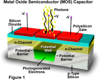
MOS capacitors are segregated into two classes of devices, one having a surface channel structure and the other having a buried channel design. It is the latter device that is used in the fabrication of modern CCDs, due to several advantages of the buried channel architecture. The MOS capacitor array is fabricated on a p-type silicon substrate (illustrated in Figure 1) in which the main charge carriers are positively charged electron "holes". Prior to the multi-step photolithography-driven CCD fabrication process, a polished silicon wafer is bombarded with boron ions to create channel stops that localize integrated charge within the confines of a single pixel gate set (not shown in Figure 1). After impregnation of the wafer with boron ions, a 10,000 angstrom layer of silicon dioxide is grown over the channel stops.
The next step in the fabrication process is to create the buried channels by implanting phosphorous ions in areas that will eventually be covered by polysilicon gate electrodes. The n-type semiconductor formed by phosphorus contains negatively charged electrons as the primary charge carriers and forms a pn-type diode structure, which serves to localize potential wells deep beneath the silicon/silicon dioxide interface. The potential well illustrated in the central portion of Figure 1 is a schematic drawing of the diode structure.
The primary function of the buried channel is to localize integrated electrons away from the silicon/silicon dioxide interface, where they can become trapped during charge transfer. By localizing charge deep within the p-type silicon substrate, transfer of charge occurs more efficiently with a minimum of residual charge remaining in the gate.
After the buried channels are formed within the silicon substrate, a layer of silicon dioxide is thermally grown on the silicon wafer surface to provide an insulating base for the gate electrodes. Next, a phosphorous-doped layer of polycrystalline silicon (polysilicon) about 5,000 angstroms thick is grown on top of the oxide layer. This layer of polysilicon comprises the gate electrodes (see Figure 1) and is transparent to visible light, making it an ideal substance for use in CCDs. Although, the fabrication of a complete CCD takes additional steps, the basics of the MOS capacitor assembly have been completed at this point.
When the capacitor is unbiased (does not have an applied voltage), electrons residing in the n-region of the device equilibrate to the lowest potential energy:
where q is the magnitude of charge density on an electron and Y is the electrostatic potential. From this equation, it follows that electrons will localize where the electrostatic potential is greatest. A potential energy diagram for the n-region is presented in Figure 2, which illustrates where the electron ensemble is congregated within the capacitor (about 1 micron beneath the oxide layer).

After a quantity of charge has been integrated by interaction with photons and a voltage is applied to the gate electrode with the silicon substrate held at ground potential, the electrostatic potential curve drawn in Figure 2 will tend to flatten at the peak. As the gate voltage is increased, the potential of electrons trapped in the buried channel rises in a linear manner.
Also illustrated in Figure 1 are neighboring gates (denoted by a -V symbol) that are biased to form barriers to the potential well created by the central gate. The MOS capacitor has the ability to move integrated charge (generated by incoming photons) by selectively changing the bias (or voltage) on the three gates relative to one another. This collection and transfer of electrons by the capacitor is the basis for the CCD image sensor.
Contributing Author
Michael W. Davidson - National High Magnetic Field Laboratory, 1800 East Paul Dirac Dr., The Florida State University, Tallahassee, Florida, 32310.
BACK TO CONCEPTS IN DIGITAL IMAGING TECHNOLOGY