
Concepts in Digital Imaging Technology
Microlens Arrays
Microlens arrays (also referred to as microlenticular arrays or lenslet arrays) are used to increase the optical fill factor in CCDs, such as interline-transfer devices, that suffer from reduced aperture due to metal shielding. These tiny lens systems serve to focus and concentrate light onto the photodiode surface instead of allowing it to fall on non-photosensitive areas of the device, where it is lost from the imaging information collected by the CCD.
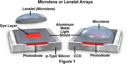
A typical lenslet placement scheme is illustrated in Figure 1, where a tiny optical lens is strategically placed over the dye layer and metal light shield of a photodiode. The lenslets are either grown in parallel arrays during the CCD fabrication process or manufactured out of a material such as quartz and placed on the array surface during packaging. Each lenslet is a high quality optical surface containing refractive elements ranging in size from several hundred to around 10 microns in diameter, depending upon the application. Lens quality is so good that microlenses are physically equivalent to an ordinary single-element lens.
Addition of microlens arrays to CCD photodiodes can increase the optical fill factor by up to three times that realized without the tiny optical components. Increasing the fill factor yields a corresponding increase in the sensitivity of the photosite. Microlens arrays provide a substantial increase in performance of interline-transfer CCD imaging arrays that have lateral overflow drains and a sizeable amount of shielded pixel space. These devices typically suffer from reduced optical fill factors because of reduced active pixel area compared to total pixel size.
| Interactive Tutorial | |||||||||||
|
|||||||||||
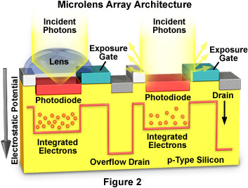
Illustrated in Figure 2 is a schematic diagram of an interline-transfer CCD pixel pair, one equipped with a microlens to concentrate light into the photodiode, while the other must absorb incident light rays without the benefit of optical assistance from a microlens. Incident photons that strike the microlens are directed into the photodiode by refraction through the glass or polymer comprising the microlens. The photodiode without a microlens collects a significantly lower portion of incoming photons, because those that impact on shielded areas (the exposure gate and neighboring structures) are not useful in charge integration. The optical fill factor of interline CCDs can be reduced to less than 20 percent by shielded vertical transfer shift registers. With the microlens array, the fill factor can approach 100 percent, depending upon manufacturing parameters.
Organization of the cone of light reaching the microlens surface depends upon the optical characteristics of the microscope or camera lens used to direct light to the CCD. Also, polysilicon gate thickness heavily influences the ability to collect light by the photodiode positioned beneath the gate structure. Microlens arrays are fabricated using reflow techniques on resist layers to achieve numerical apertures ranging from 0.15 to 0.4 with short focal lengths and corresponding lens diameters of 20 to 800 microns. The fill factor of a microlens array is strongly dependent upon the manufacturing process used to create the array. Glass lenses of somewhat lower (0.05 to 0.2) numerical aperture are also utilized. Lower numerical aperture microlenses have fewer optical aberrations with significantly longer focal lengths.
Disadvantages encountered with microlenses are far outweighed by increased sensitivity of devices having these optical components in place. One of the primary difficulties occurs when light rays from the outer portions of a pixel are focused onto an adjacent lens (and subsequently onto the detector photodiode) resulting in mis-registration. In addition, when detector pixel size reaches the diffraction limit of the microlenses, the pixels become overfilled leading to inaccurate measurements. As photodiodes become smaller, the problems associated with producing quality microlenses increase. Higher quality microlenses are needed to produce images on these arrays, but spherical aberration then becomes a problem. Adding microlenses to CCDs increases the number of processing steps, and the uniformity of the lens array is a variable that can often cause problems during fabrication.
Contributing Authors
Mortimer Abramowitz - Olympus America, Inc., Two Corporate Center Drive., Melville, New York, 11747.
Michael W. Davidson - National High Magnetic Field Laboratory, 1800 East Paul Dirac Dr., The Florida State University, Tallahassee, Florida, 32310.
BACK TO CONCEPTS IN DIGITAL IMAGING TECHNOLOGY