Introduction to Light Emitting Diodes
The past few decades have brought a continuing and rapidly evolving sequence of technological revolutions, particularly in the digital arena, which has dramatically changed many aspects of our daily lives. The developing race among manufacturers of light emitting diodes (LEDs) promises to produce, literally, the most visible and far-reaching transition to date. Recent advances in the design and manufacture of these miniature semiconductor devices may result in the obsolescence of the common light bulb, perhaps the most ubiquitous device utilized by modern society.
The incandescent lamp is the best known of Thomas Edison's major inventions, and the only one to have persisted in use (and in nearly its original form) to the present day, now more than a century after its introduction. The phonograph, tickertape, and mimeograph machines have been replaced by digital technologies in the last few decades, and recently, full-spectrum light emitting diode devices are becoming widespread, and could force incandescent and fluorescent lamps into extinction. While some applications of LED technology may be as straightforward as replacing one light bulb with another, far more visionary changes may involve dramatic new mechanisms for utilizing light. As a result of the predicted evolution, walls, ceilings, or even entire buildings could become the targets for specialized lighting scenarios, and interior design changes might be accomplished through illumination effects rather than by repainting or refurnishing. At the very least, a widespread change from incandescent to LED illumination would result in enormous energy savings.
Although light emitting diodes are in operation all around us in videocassette recorders, clock radios, and microwave ovens, for example, their use has been limited mainly to display functions on electronic appliances. The tiny red and green indicator lights on computers and other devices are so familiar, the fact that the first LEDs were limited to a dim red output is probably not widely recognized. In fact, even the availability of green-emitting diodes represented a significant developmental step in the technology. In the past 15 years or so, LEDs have become much more powerful, and available in a wide spectrum of colors. A breakthrough that enabled fabrication of the first blue LED in the early 1990s, emitting light at the opposite end of the visible light spectrum from red, opened up the possibility to create virtually any color of light. More important, the discovery made it technically feasible to produce white light from the tiny semiconductor devices. An inexpensive, mass-market version of white LED is the most sought-after goal of researchers and manufacturers, and is the device most likely to end a hundred-year reliance on inefficient incandescent lamps.
The widespread utilization of diode devices for general lighting is still some years away, but LEDs are beginning to replace incandescent lamps in many applications. There are a number of reasons for replacing conventional incandescent light sources with modern semiconductor alternatives. Light emitting diodes are far more efficient than incandescent bulbs at converting electricity into visible light, they are rugged and compact, and can often last 100,000 hours in use, or about 100 times longer than incandescent bulbs. LEDs are fundamentally monochromatic emitters, and applications requiring high-brightness, single-color lamps are experiencing the greatest number of applications within the current generation of improved devices. The use of LEDs is increasing for automotive taillights, turn signals, and side marker lights. As one of the first automotive applications, the high-mount brake light on cars and trucks is a particularly appealing location for incorporating LEDs. Long LED lifespans allow manufacturers more freedom to integrate the brake light into the vehicle design without the necessity of providing for frequent (and easy) replacement, as is required when incandescent bulbs are used.
Approximately 10 percent of the red traffic lights in the United States have now been replaced with LED-based lamps. The higher initial cost of the LEDs can be recovered in as little as one year, due to their higher efficiency in producing red light, which is accomplished without the need for filtering. The LEDs in a red traffic light consume about 10 to 25 watts, compared with 50 to 150 for a red-filtered incandescent light of similar brightness. The longevity of the LEDs is an obvious advantage in reducing expensive maintenance of the signals. Single-color LEDs are also being utilized as runway lights at airports and as warning lights on radio and television transmission towers.
As improvements have been made in manufacturing efficiency and toward the ability to produce light emitting diodes with virtually any output color, the primary focus of researchers and industry has become the white light diode. Two primary mechanisms are being employed to produce white light from devices that are fundamentally monochromatic, and both techniques will most likely continue to be utilized for different applications. One method involves mixing different colors of light from multiple LEDs, or from different materials in a single LED, in proportions that result in light that appears white. The second technique relies on using LED emission (commonly non-visible ultraviolet) to provide energy for excitation of another substance, such as a phosphor, which in turn produces white light. Each method has both advantages and disadvantages that are likely to be in constant flux as further developments occur in LED technology.
Fundamentals of Semiconductor Diodes
Details of the fundamental processes underlying the function of light emitting diodes, and the materials utilized in their construction, are presented in the ensuing discussion. The basic mechanism by which LEDs produce light can be summarized, however, by a simple conceptual description. The familiar light bulb relies upon temperature to emit visible light (and significantly more invisible radiation in the form of heat) through a process known as incandescence. In contrast, the light emitting diode employs a form of electroluminescence, which results from the electronic excitation of a semiconductor material. The basic LED consists of a junction between two different semiconductor materials (illustrated in Figure 2), in which an applied voltage produces a current flow, accompanied by the emission of light when charge carriers injected across the junction are recombined.
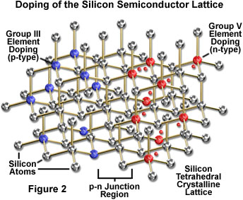
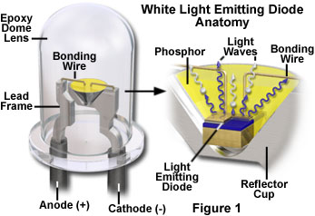
The fundamental element of the LED is a semiconductor chip (similar to an integrated circuit), which is mounted in a reflector cup supported by a lead frame connected to two electrical wires, and then embedded in a solid epoxy lens (see Figure 1). One of the two semiconductor regions that comprise the junction in the chip is dominated by negative charges (n-type region; Figure 2)), and the other is dominated by positive charges (p-type region). When a sufficient voltage is applied to the electrical leads, current flows and electrons move across the junction from the n region into the p region where the negatively charged electrons combine with positive charges. Each combination of charges is associated with an energy level reduction that may release a quantum of electromagnetic energy in the form of a light photon. The frequency, and perceived color, of emitted photons is characteristic of the semiconductor material, and consequently, different colors are achieved by making changes in the semiconductor composition of the chip.
The functional details of the light emitting diode are based on properties common to semiconductor materials, such as silicon, which have variable conduction characteristics. In order for a solid to conduct electricity, its resistance must be low enough for electrons to move more or less freely throughout the bulk of the material. Semiconductors exhibit electrical resistance values intermediate between those of conductors and insulators, and their behavior can be modeled in terms of the band theory for solids. In a crystalline solid, electrons of the constituent atoms occupy a large number of energy levels that may differ very little either in energy or in quantum number. The wide spectrum of energy levels tend to group together into nearly continuous energy bands, the width and spacing of which differ considerably for different materials and conditions.
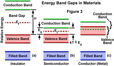
At progressively higher energy levels, proceeding outward from the nucleus, two distinct energy bands can be defined, which are termed the valence band and the conduction band (Figure 3). The valence band consists of electrons at a higher energy level than the inner electrons, and these have some freedom to interact in pairs to form a type of localized bond among atoms of the solid. At still-higher energy levels, electrons of the conduction band behave similarly to electrons in individual atoms or molecules that have been excited above ground state, with a high degree of freedom to move about within the solid. The difference in energy between the valence and conduction bands is defined as the band gap for a particular material.
In conductors, the valence and conduction bands partially overlap in energy (see Figure 3), so that a portion of the valence electrons always resides in the conduction band. The band gap is essentially zero for these materials, and with part of the valence electrons moving freely into the conduction band, vacancies or holes occur in the valence band. Electrons move, with very little energy input, into holes in bands of adjacent atoms, and the holes migrate freely in the opposite direction. In contrast to these materials, insulators have fully occupied valence bands and larger band gaps, and the only mechanism by which electrons can move from atom to atom is for a valence electron to be displaced into the conduction band, requiring a large energy expenditure.
Semiconductors have band gaps that are small but finite, and at normal temperatures, thermal agitation is sufficient to move some electrons into the conduction band where they can contribute to electrical conduction. Resistance can be reduced by increasing the temperature, but many semiconductor devices are designed in such a manner that the application of a voltage produces the required changes in electron distribution between the valence and conduction bands to enable current flow. Although the band arrangement is similar for all semiconductors, there are large differences in the band gap (and in the distribution of electrons among the bands) at specific temperature conditions.
The element silicon is the simplest intrinsic semiconductor, and is often used as a model for describing the behavior of these materials. In its pure form, silicon does not have sufficient charge carriers, or appropriate band gap structure, to be useful in light emitting diode construction, but is widely used to fabricate other semiconductor devices. The conduction characteristics of silicon (and other semiconductors) can be improved through the introduction of impurities in small quantities to the crystal, which serve to provide either additional electrons or vacancies (holes) in the structure. Through this process, referred to as doping, producers of integrated circuits have developed considerable ability to tailor the properties of semiconductors to suit specific applications.
The process of doping to modify the electronic properties of semiconductors is most easily understood by considering the relatively simple silicon crystal structure. Silicon is a Group IV member of the periodic table, having four electrons that may participate in bonding with neighboring atoms in a solid. In pure form, each silicon atom shares electrons with four neighbors, with no deficit or excess of electrons beyond those required in the crystal structure. If a small amount of a Group III element (those having three electrons in their outermost energy level) is added to the silicon structure, an insufficient number of electrons exist to satisfy the bonding requirements. The electron deficiency creates a vacancy, or hole, in the structure, and the resulting positive electrical character classifies the material as p-type. Boron is one of the elements that is commonly utilized to dope pure silicon to achieve p-type characteristics.
Doping in order to produce the opposite type of material, having a negative overall charge character (n-type), is accomplished through the addition of Group V elements, such as phosphorus, which have an "extra" electron in their outermost energy level. The resulting semiconductor structure has an excess of available electrons over the number required for covalent silicon bonding, which bestows the ability to act as an electron donor (characteristic of n-type material).
Although silicon and germanium are commonly employed in semiconductor fabrication, neither material is suitable for light emitting diode construction because junctions employing these elements produce a significant amount of heat, but only a small quantity of infrared or visible light emission. Photon-emitting diode p-n junctions are typically based on a mixture of Group III and Group V elements, such as gallium arsenide, gallium arsenide phosphide, and gallium phosphide. Careful control of the relative proportions of these compounds, and others incorporating aluminum and indium, as well as the addition of dopants such as tellurium and magnesium, enables manufacturers and researchers to produce diodes that emit red, orange, yellow, or green light. Recently the use of silicon carbide and gallium nitride has permitted blue-emitting diodes to be introduced, and combining several colors in various combinations provides a mechanism to produce white light. The nature of materials comprising p-type and n-type sides of the device junction, and the resulting energy band structure, determines the energy levels that are available during charge recombination in the junction region, and therefore, the magnitude of the energy quanta released as photons. As a consequence, the color of light emitted by a particular diode depends upon the structure and composition of the p-n junction.
The fundamental key to manipulating properties of solid-state electronic devices is the nature of the p-n junction. When dissimilar doped materials are placed in contact with each other, the flow of current in the region of the junction is different than it is in either of the two materials alone. Current will readily flow in one direction across the junction, but not in the other, constituting the basic diode configuration. This behavior can be understood in terms of the movement of electrons and holes in the two material types and across the junction. The extra free electrons in the n-type material tend to move from the negatively charged area to a positively charged area, or toward the p-type material. In the p-type region, which has vacant electron sites (holes), lattice electrons can jump from hole to hole, and will tend to move away from the negatively charged area. The result of this migration is that the holes appear to move in the opposite direction, or away from the positively charged region and toward the negatively charged area (Figure 4). Electrons from the n-type region and holes from the p-type region recombine in the vicinity of the junction to form a depletion zone (or layer), in which no charge carriers remain. In the depletion zone, a static charge is established that inhibits any additional electron transfer, and no appreciable charge can flow across the junction unless assisted by an external bias voltage.
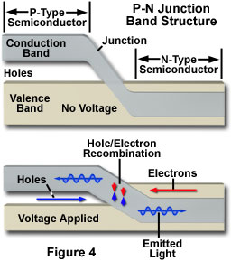
In a diode configuration, electrodes on opposite ends of the device enable a voltage to be applied in a manner that can overcome the effect of the depletion region. Connecting the n-type region of the diode to the negative side of an electrical circuit, and the p-type region to the positive side will cause electrons to move from the n-type material toward the p-type, and holes to move in the opposite direction. With application of a sufficiently high voltage, the electrons in the depletion region are elevated in energy to dissociate with the holes, and to begin moving freely again. Operated with this circuit polarity, referred to as forward biasing of the p-n junction, the depletion zone disappears and charge can move across the diode. Holes are driven to the junction from the p-type material and electrons are driven to the junction from the n-type material. The combination of holes and electrons at the junction allows a continuous current to be maintained across the diode.
If the circuit polarity is reversed with respect to the p-type and n-type regions, electrons and holes will be pulled in opposite directions, with an accompanying widening of the depletion region at the junction. No continuous current flow occurs in a reverse-biased p-n junction, although initially a transient current will flow as the electrons and holes are pulled away from the junction. Current flow will cease as soon as the growing depletion zone creates a potential that is equal to the applied voltage.
Light Emitting Diode Construction
Manipulation of the interaction between electrons and holes at the p-n junction is fundamental in the design of all semiconductor devices, and for light emitting diodes, the primary design goal is the efficient generation of light. Injection of carriers across the p-n junction is accompanied by a drop in electron energy levels from the conduction band to lower orbitals. This process takes place in any diode, but only produces visible light photons in those having specific material compositions. In a standard silicon diode, the energy level difference is relatively small, and only low frequency emission occurs, predominately in the infrared region of the spectrum. Infrared diodes are useful in many devices, including remote controls, but the design of visible-light emitting diodes requires fabrication with materials exhibiting a wider gap between the conduction band and orbitals of the valence band. All semiconductor diodes release some form of light, but most of the energy is absorbed into the diode material itself unless the device is specifically designed to release the photons externally. In addition, to be useful as a light source, diodes must concentrate light emission in a specific direction. Both the composition and construction of the semiconductor chip, and the design of the LED housing, contribute to the nature and efficiency of energy emission from the device.
The basic structure of a light emitting diode consists of the semiconductor material (commonly referred to as a die), a lead frame on which the die is placed, and the encapsulation epoxy surrounding the assembly (see Figure 1). The LED semiconductor chip is supported in a reflector cup coined into the end of one electrode (the cathode), and, in the typical configuration, the top face of the chip is connected with a gold bonding wire to a second electrode (anode). Several junction structure designs require two bonding wires, one to each electrode. In addition to the obvious variation in the radiation wavelength of different LEDs, there are variations in shape, size, and radiation pattern. The typical LED semiconductor chip measures approximately 0.25 millimeter-square, and the epoxy body ranges from 2 to about 10 millimeters in diameter. Most commonly, the body of the LED is round, but they may be rectangular, square, or triangular.
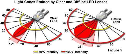
Although the color of light emitted from a semiconductor die is determined by the combination of chip materials, and the manner in which they are assembled, certain optical characteristics of the LED can be controlled by other variables in the chip packaging. The beam angle can be narrow or wide (see Figure 5), and is determined by the shape of the reflector cup, the size of the LED chip, the distance from chip to the top of the epoxy housing or lens, and the geometry of the epoxy lens. The tint of the epoxy lens does not determine the emission color of the LED, but is often used as a convenient indicator of the lamp's color when it is inactive. LEDs intended for applications that require high intensity, and no color in the off-state, have clear lenses with no tint or diffusion. This type produces the greatest light output, and may be designed to have the narrowest beam, or viewing angle. Non-diffused lenses typically exhibit viewing angles of plus or minus 10 to 12 degrees (Figure 5). Their intensity allows them to be utilized for backlighting applications, such as the illumination of display panels on electronic devices.
For creation of diffused LED lenses, minute glass particles are embedded in the encapsulating epoxy. The diffusion created by inclusion of the glass spreads light emitted by the diode, producing a viewing angle of approximately 35 degrees on either side of the central axis. This lens style is commonly employed in applications in which the LED is viewed directly, such as for indicator lamps on equipment panels.
The choice of material systems and fabrication techniques in LED construction is guided by two primary goals�maximization of light generation in the chip material, and the efficient extraction of the generated light. In the forward-biased p-n junction, holes are injected across the junction from the p region into the n region, and electrons are injected from the n region into the p region. The equilibrium charge carrier distribution in the material is altered by this injection process, which is referred to as minority-carrier injection. Recombination of minority carriers with majority carriers takes place to reestablish thermal equilibrium, and continued current flow maintains the minority-carrier injection. When the recombination rate is equal to the injection rate, a steady-state carrier distribution is established. Minority-carrier recombination can take place in a radiative fashion, with the emission of a photon, but for this to occur the proper conditions must be established for energy and momentum conservation. Meeting these conditions is not an instantaneous process, and a time delay results before radiative recombination of the injected minority carrier can take place. This delay, the minority carrier lifetime, is one of the primary variables that must be considered in LED material design.
Although the radiative recombination process is desirable in LED design, it is not the only recombination mechanism that is possible in semiconductors. Semiconductor materials cannot be produced without some impurities, structural dislocations, and other crystalline defects, and these can all trap injected minority carriers. Recombinations of this type may or may not produce light photons. Recombinations that do not produce radiation are slowed by the diffusion of the carriers to suitable sites, and are characterized by a nonradiative process lifetime, which can be compared to the radiative process lifetime.
An obvious goal in LED design, given the factors just described, is to maximize the radiative recombination of charge carriers relative to the nonradiative. The relative efficiency of these two processes determines the fraction of injected charge carriers that combine radiatively compared to the total number injected, which can be stated as the internal quantum efficiency of the material system. The choice of materials for LED fabrication relies upon an understanding of semiconductor band structure and the means by which the energy levels can be chosen or manipulated to produce favorable quantum efficiency values. Interestingly, certain groups of III-V compounds have internal quantum efficiencies of nearly 100 percent, while other compounds utilized in semiconductors may have internal quantum efficiencies as low as 1 percent.
The radiative lifetime for a particular semiconductor largely determines whether radiative recombinations occur before nonradiative. Most semiconductors have similar simple valence band structure with an energy peak situated around a particular crystallographic direction, but with much more variation in the structure of the conduction band. Energy valleys exist in the conduction band, and electrons occupying the lowest-energy valleys are positioned to more easily participate in recombination with minority carriers in the valence band. Semiconductors can be classified as direct or indirect depending upon the relative positioning of the conduction band energy valleys and the energy apex of the valence band in energy/momentum space. Direct semiconductors have holes and electrons positioned directly adjacent at the same momentum coordinates, so that electrons and holes can recombine relatively easily while maintaining momentum conservation. In an indirect semiconductor, the match between conduction band energy valleys and holes that would allow momentum conservation is not favorable, most of the transitions are forbidden, and the resulting radiative lifetime is long.
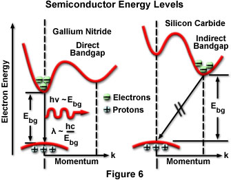
Silicon and germanium are examples of indirect semiconductors, in which radiative recombination of injected carriers is extremely unlikely. The radiative lifetime in such materials occurs in the range of seconds, and nearly all injected carriers combine nonradiatively through defects in the crystal. Direct semiconductors, such as gallium nitride or gallium arsenide, have short radiative lifetimes (approximately 1 to 100 nanoseconds), and materials can be produced with sufficiently low defect density that radiative processes are as likely as nonradiative. For a recombination event to occur in indirect gap materials, an electron must change its momentum before combining with a hole, resulting in a significantly lower recombination probability for the occurrence of a band-to-band transition. The quantum efficiencies exhibited by LEDs constructed of the two types of semiconductor material clearly reflect this fact. Gallium nitride LEDs have quantum efficiencies as high as 12 percent, compared to the 0.02 percent typical of silicon carbide LEDs. Figure 6 presents an energy band diagram for direct band gap GaN and indirect band gap SiC that illustrates the nature of the band-to-band energy transition for the two types of material.
The wavelength (and color) of light emitted in a radiative recombination of carriers injected across a p-n junction is determined by the difference in energy between the recombining electron-hole pair of the valence and conduction bands. The approximate energies of the carriers correspond to the upper energy level of the valence band and the lowest energy of the conduction band, due to the tendency of the electrons and holes to equilibrate at these levels. Consequently, the wavelength (l) of an emitted photon is approximated by the following expression:
where h represents Planck's constant, c is the velocity of light, and E(bg) is the band gap energy. In order to change the wavelength of emitted radiation, the band gap of the semiconducting material utilized to fabricate the LED must be changed. Gallium arsenide is a common diode material, and may be used as an example illustrating the manner in which a semiconductor's band structure can be altered to vary the emission wavelength of the device. Gallium arsenide has a band gap of approximately 1.4 electron-volts, and emits in the infrared at a wavelength of 900 nanometers. In order to increase the frequency of emission into the visible red region (about 650 nanometers), the band gap must be increased to approximately 1.9 electron-volts. This can be achieved by mixing gallium arsenide with a compatible material having a larger band gap. Gallium phosphide, having a band gap of 2.3 electron-volts, is the most likely candidate for this mixture. LEDs produced with the compound GaAsP (gallium arsenide phosphide) can be customized to produce band gaps of any value between 1.4 and 2.3 electron-volts, through adjustment of the content of arsenic to phosphorus.
As previously discussed, maximization of light generation in the diode semiconductor material is a primary design goal in LED fabrication. Another requirement is the efficient extraction of the light from the chip. Because of total internal reflection, only a fraction of the light that is generated isotropically within the semiconductor chip can escape to the outside. According to Snell's law, light can travel from a medium of higher refractive index into a medium of lower refractive index only if it intersects the interface between the two media at an angle less than the critical angle for the two media. In a typical light-emitting semiconductor having cubic shape, only about 1 to 2 percent of the generated light escapes through the top surface of the LED (depending upon the specific chip and p-n junction geometry), the remainder being absorbed within the semiconductor materials.
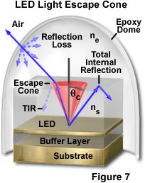
Figure 7 illustrates the escape of light from a layered semiconductor chip of refractive index n(s) into epoxy of lower index (n(e)). The angle subtended by the escape cone is defined by the critical angle, q(c), for the two materials. Light rays emerging from the LED at angles less than q(c) escape into the epoxy with minimal reflection loss (dashed ray lines), while those rays propagating at angles greater than q(c) undergo total internal reflection at the boundary, and do not escape the chip directly. Because of the curvature of the epoxy dome, most light rays leaving the semiconductor material meet the epoxy/air interface at nearly right angles, and emerge from the housing with little reflection loss.
The proportion of light emitted from an LED chip into the surroundings is dependent upon the number of surfaces through which light can be emitted, and how effectively this occurs at each surface. Nearly all LED structures rely on some form of layered arrangement in which epitaxial growth processes are utilized to deposit several lattice-matched materials on top of one another to tailor the properties of the chip. A wide variety of structures is employed, with each material system requiring different layer architecture in order to optimize performance properties.
Most of the LED structural arrangements rely on a secondary growth step to deposit a single-crystal layer on top of a single-crystal bulk-grown substrate material. Such a multilayering approach enables designers to satisfy seemingly contradictory or inconsistent requirements. A common feature of all of the structural types is that the p-n junction, where the light emission occurs, is almost never located in the bulk-grown substrate crystal. One reason for this is that bulk-grown material generally has a high defect density, which lowers the light generation efficiency. In addition, the most common bulk-grown materials, including gallium arsenide, gallium phosphide, and indium phosphide, do not have the appropriate band gap for the desired emission wavelengths. Another requirement in many LED applications is for a low series resistance that can be met by appropriate substrate choice, even in cases in which the low doping required in the p-n junction region would not provide adequate conduction.
The techniques of epitaxial crystal growth involve deposition of one material on another, which is closely matched in atomic lattice constants and thermal expansion coefficient to reduce defects in the layered material. A number of techniques are in use to produce epitaxial layers. These include Liquid Phase Epitaxy (LPE), Vapor Phase Epitaxy (VPE), Metal-Organic Epitaxial Chemical Vapor Deposition (MOCVD), and Molecular Beam Epitaxy (MBE). Each of the growth techniques has advantages in particular materials systems or production environments, and these factors are extensively discussed in the literature.
The details of the various epitaxial structures employed in LED fabrication are not presented here, but are discussed in a number of publications. Generally, however, the most common categories of such structures are grown and diffused homojunctions, and single confinement or double confinement heterojunctions. The strategies behind the application of the various layer arrangements are numerous. These include structuring of p and n regions and reflective layers to increase the internal quantum efficiency of the system, graded-composition buffer layers to overcome lattice mismatch between layers, locally varying energy band gap to accomplish carrier confinement, and lateral constraint of carrier injection to control light emission area or to collimate the emission.
Even though it does not typically contain the p-n junction region, the LED substrate material becomes an integral part of the function, and is chosen to be appropriate for deposition of the desired epitaxial layers, as well as for its light transmission and other properties. As previously stated, the fraction of generated light that is actually emitted from an LED chip is a function of the number of surfaces that effectively transmit light. Most LED chips are categorized as absorbing substrate (AS) devices, where the substrate material has a narrow band gap and absorbs all emission having energy greater than the band gap. Therefore, light traveling toward the sides or downward is absorbed, and such chips can only emit light through their top surfaces.
The transparent substrate (TS) chip is designed to increase light extraction by incorporating a substrate that is transparent to the wavelength of emitted light. In some systems, transparency in the upper epitaxial layers will allow light transmitted toward the side surfaces, within certain angles, to be extracted as well. Hybrid designs, having substrate properties intermediate between AS and TS devices, are also utilized, and significant increases in extraction efficiency can be achieved by employment of a graded change in refractive index from the LED chip to air. There remain numerous other absorption mechanisms in the LED structure that reduce emission and are difficult to overcome, such as the front and back contacts on the chip, and crystal defects. However, chips made on transparent, as opposed to absorbing, substrates can exhibit a nearly-fivefold improvement in extraction efficiency.
Development of Multiple LED Colors
The first commercial light emitting diode, developed in the 1960s, utilized the primary constituents gallium, arsenic, and phosphorus to produce red light (655-nanometer wavelength). An additional red light-emitting material, gallium phosphide, was later used to produce diodes emitting 700-nanometer light. The latter version has seen limited application, in spite of high efficiency, due to the low apparent brightness resulting from relative insensitivity of the human eye in that spectral region. Throughout the 1970s, technological developments enabled additional diode colors to be introduced, and production improvements increased the quality control and reliability of the devices.
Changes in the elemental proportions, doping, and substrate materials resulted in development of gallium-arsenide-phosphorus (GaAsP) diodes producing orange and yellow emission, as well as a higher-efficiency red emitter. Green diodes based on GaP chips were also developed. The introduction and refinement of the use of gallium-aluminum-arsenide (GaAlAs), during the 1980s, resulted in a rapid growth in the number of applications for light emitting diodes, largely due to an order-of-magnitude improvement in brightness compared to previous devices. This gain in performance was achieved by the use of multilayer heterojunction structures in the chip fabrication, and although these GaAlAs diodes are limited to emission in the red (660 nanometers), they began to be used in outdoor signs, bar code scanners, medical equipment, and fiber optic data transmission.
Light Emitting Diode Color Variations
|
||||||||||||||||||||||||||||||||||||||||||||
Table 1
A major development occurred in the late 1980s, when LED designers borrowed techniques from the rapidly progressing laser diode industry, leading to the production of high-brightness visible light diodes based on the indium-gallium-aluminum-phosphide (AlGaInP) system. This material allows changes in the emission color by adjustment of the band gap. Therefore, the same production techniques can be employed to produce red, orange, yellow, and green LEDs. Table 1 lists many of the common LED chip materials (epitaxial layers and, in some cases, the substrate) and their emission wavelengths (or corresponding color temperature for white light LEDS).
More recently, blue LEDs have been developed based on gallium nitride and silicon carbide materials. Production of light in this shorter-wavelength, more energetic region of the visible spectrum, has long been elusive to designers of LEDs. High photon energies typically increase the failure rate of semiconductor devices, and the low sensitivity of the human eye to blue light adds to the brightness requirement for a useful blue diode. One of the most important aspects of a blue light emitting diode is that it completes the red, green, and blue (RGB) primary color family to provide an additional mechanism of producing solid-state white light, through the mixing of these component colors.
Solid-state researchers have sought to develop a bright blue light source since the development of the first light emitting diodes. Although LEDs utilizing silicon carbide can produce blue light, they have extremely low luminous efficiency, and are not capable of producing the brightness that is necessary for practical applications. Recent developments in Group III-nitride based semiconductors have led to a revolution in diode technology. In particular, the gallium-indium-nitride (GaInN) system has emerged as the leading candidate for the production of blue LEDs, and is also a primary material in the developing white LED market. The GaInN material system evolved in the 1990s with the achievement of p-doping in GaN, followed later by the utilization of GaInN/GaN double heterostructure for LED fabrication, and then by the commercial availability of high-brightness blue and green GaInN LEDs in the late 1990s.
White Light LEDs
The role of the gallium-indium-nitride semiconductor material system extends to the development of white-light diodes. The addition of bright blue-emitting LEDs to the earlier-developed red and green devices makes it possible to use three LEDs, tuned to appropriate output levels, to produce any color in the visible light spectrum, including white. Other possible approaches to producing white light, utilizing a single device, are based on phosphor or dye wavelength converters or semiconductor wavelength converters. The concept of a white LED is particularly attractive for general illumination, due to the reliability of solid-state devices, and the potential for delivering very high luminous efficiency compared to conventional incandescent and fluorescent sources.
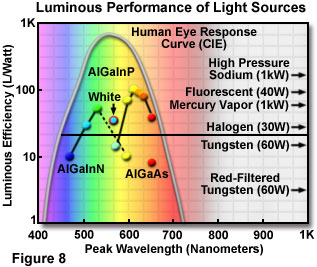
Whereas conventional light sources exhibit an average output of 15 to 100 lumens per watt, the efficiency of white LEDs is predicted to reach more than 300 lumens per watt through continued development. Figure 8 illustrates the luminous efficiency values for a number of LED types and conventional light sources, and includes the CIE (Commission Internationale de l'Eclairage) luminosity curve for the visible wavelength range. This curve represents the human eye response to an emitter of 100 percent efficiency. Some of the current LED materials systems exhibit higher luminous performance than most of the conventional light sources, and soon light emitting diodes are expected to be the most efficient emitters available.
White LEDs are certainly suitable for display and signage applications, but in order to be useful for general illumination (as hoped), and for applications demanding accurate and aesthetically pleasing color rendering (including illumination for optical microscopy), the manner in which "white" light is achieved must be seriously considered. The human eye perceives light as being white if the three types of photosensory cone cells, located in the retina, are stimulated in particular ratios. The three cone types exhibit response curves that peak in sensitivity at wavelengths representing red, green, and blue, and the combination of response signals produces various color sensations in the brain. A wide variety of different color mixtures are capable of producing a similar perceived color, especially in the case of white, which may be realized through many combinations of two or more colors.
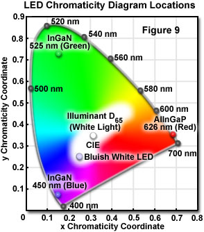
A chromaticity diagram is a graphical means of representing the results obtained from mixing colors. Monochromatic colors appear on the periphery of the diagram, and a range of mixtures representing white is located in the central region of the diagram (see Figure 9). Light that is perceived as white can be generated by different mechanisms. One method is to combine light of two complementary colors in the proper power ratio. The ratio that produces a tristimulus response in the retina (causing the perception of white) varies for different color combinations. A selection of complementary wavelengths are listed in Table 2, along with the power ratio for each pair that produces the chromaticity coordinates of a standard illuminant designated as D(65) by the International Commission for Illumination (CIE, Commission Internationale de l'Eclairage).
Another means of generating white light is by combining the emission of three colors that will produce the perception of white light when they are combined in the proper power ratio. White light can also be produced by broadband emission from a substance that emits over a large region of the visible spectrum. This type of emission approximates sunlight, and is perceived as white. Additionally, broadband emission can be combined with emission at discrete spectral lines to produce a perceived white, which may have particular desirable color characteristics that differ from those of white light produced by other techniques.
The combination of red, green, and blue diode chips into one discrete package, or in a lamp assembly housing a cluster of diodes, allows the generation of white light or any of 256 colors by utilizing circuitry that drives the three diodes independently. In applications requiring a full spectrum of colors from a single point source, this type of RGB diode format is the preferred technique.
Most white-light diodes employ a semiconductor chip emitting at a short wavelength (blue, violet or ultraviolet) and a wavelength converter, which absorbs light from the diode and undergoes secondary emission at a longer wavelength. Such diodes, therefore, emit light of two or more wavelengths, that when combined, appear as white. The quality and spectral characteristics of the combined emission vary with the different design variations that are possible. The most common wavelength converter materials are termed phosphors, which exhibit luminescence when they absorb energy from another radiation source. The typically utilized phosphors are composed of an inorganic host substance containing an optically active dopant. Yttrium aluminum garnet (YAG) is a common host material, and for diode applications, it is usually doped with one of the rare-earth elements or a rare-earth compound. Cerium is a common dopant element in YAG phosphors designed for white light emitting diodes.
Complementary Color Wavelengths
|
||||||||||||||||||||||||||||||||
Table 2
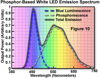
The first commercially available white LED (fabricated and distributed by the Nichia Corporation) was based on a blue-light-emitting gallium-indium-nitride (GaInN) semiconductor device surrounded by a yellow phosphor. Figure 1 illustrates the cross-sectional structure of the device. The phosphor is Ce-doped YAG, produced in powder form and suspended in the epoxy resin used to encapsulate the die. The phosphor-epoxy mixture fills the reflector cup that supports the die on the lead frame, and a portion of the blue emission from the chip is absorbed by the phosphor and reemitted at the longer phosphorescence wavelength. The combination of the yellow photo-excitation under blue illumination is ideal in that only one converter species is required. Complementary blue and yellow wavelengths combine through additive mixing to produce the desired white light. The resulting emission spectrum of the LED (Figure 10) represents the combination of phosphor emission, with the blue emission that passes through the phosphor coating unabsorbed.
The relative contributions of the two emission bands can be modified to optimize the luminous efficiency of the LED, and the color characteristics of the total emission. These adjustments can be accomplished by changing the thickness of the phosphor-containing epoxy surrounding the die, or by varying the concentration of the phosphor suspended in the epoxy. The bluish white emission from the diode is synthesized, in effect, by additive color mixing, and its chromaticity characteristics are represented by a central location (0.25, 0.25) on the CIE chromaticity diagram (Figure 9; Bluish White LED).
White light diodes can generate emission by another mechanism, utilizing broad-spectrum phosphors that are optically excited by ultraviolet radiation. In such devices, an ultraviolet-emitting diode is employed to transfer energy to the phosphor, and the entire visible emission is generated by the phosphor. Phosphors that emit at a broad range of wavelengths, producing white light, are readily available as the materials used in fluorescent light and cathode ray tube manufacture. Although fluorescent tubes derive their ultraviolet emission from a gas discharge process, the phosphor emission stage producing white light output is the same as in ultraviolet-pumped white diodes. The phosphors have well known color characteristics and diodes of this type have the advantage that they can be designed for applications requiring critical color rendering. A significant disadvantage of the ultraviolet-pumped diodes, however, is their lower luminous efficiency when compared to white diodes employing blue light for phosphor excitation. This results from the relatively high energy loss in the down-conversion of ultraviolet light to longer visible wavelengths.
Dyes are another suitable type of wavelength converter for white diode applications, and can be incorporated into the epoxy encapsulant or in transparent polymers. The commercially available dyes are generally organic compounds, which are chosen for a specific LED design by consideration of their absorption and emission spectra. The light generated by the diode must match the absorption profile of the converting dye, which in turn emits light at the desired longer wavelength. The quantum efficiencies of dyes can be near 100 percent, as in phosphor conversion, but they have the disadvantage of poorer long-term operational stability than phosphors. This is a serious drawback, as the molecular instability of the dyes causes them to lose optical activity after a finite number of absorptive transitions, and the resulting change in light emitting diode color will limit its lifetime.
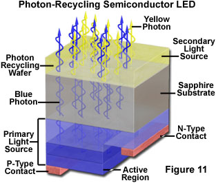
White light LEDs based on semiconductor wavelength converters have been demonstrated that are similar in principle to the phosphor conversion types, but which employ a second semiconductor material that emits a different wavelength in response to the emission from the primary source wafer. These devices have been referred to as photon recycling semiconductors (or PRS-LEDs), and incorporate a blue-emitting LED die bonded to another die that responds to the blue light by emitting light of a complementary wavelength. The two wavelengths then combine to produce white. One possible structure for this type of device utilizes a GaInN diode as a current-injected active region coupled to an AlGaInP optically-excited active region. The blue light emitted by the primary source is partially absorbed by the secondary active region, and "recycled" as reemitted photons of lower energy. The structure of a photon recycling semiconductor is illustrated schematically in Figure 11. In order for the combined emission to produce white light, the intensity ratio of the two sources must have a specific value that can be calculated for the particular dichromatic components. The choice of materials and the thickness of the various layers in the structure can be modified to vary the color of the device output.
Because white light can be created by several different mechanisms, utilizing white LEDs in a particular application requires consideration of the suitability of the method employed to generate the light. Although the perceived color of light emitted by various techniques may be similar, its effect on color rendering, or the result of filtration of the light, for example, may be entirely different. White light created through broadband emission, through mixing of two complementary colors in a dichromatic source, or by mixing of three colors in a trichromatic source, can be located at different coordinates on the chromaticity diagram and have different color temperatures with respect to illuminants designated as standards by the CIE. It is important to realize, however, that even if different illuminants have identical chromaticity coordinates, they may still have substantially different color rendering properties (Table 3), due to variations in details of each source's output spectrum.
LED Efficiency and Color Rendering Index
|
||||||||||||||||||||||
Table 3
Two factors, referred to previously, are of primary importance in evaluating white light generated by LEDs: the luminous efficiency, and the color rendering capabilities. A property referred to as the color rendering index (CRI) is utilized in photometry to compare light sources, and is defined as the source's color rendering ability with respect to that of a standard reference illumination source. It can be demonstrated that there exists a fundamental trade-off between luminous efficiency and color rendering ability of light-emitting devices, as illustrated by the values in Table 3. For an application such as signage, which utilize blocks of monochromatic light, the luminous efficiency is of primary importance, while the color rendering index is irrelevant. For general illumination, both factors must be optimized.
The spectral nature of the illumination emitted from a device has a profound influence on its color rendering ability. Although the highest possible luminous efficiency can be obtained by mixing two monochromatic complementary colors, such a dichromatic light source has a low color rendering index. In a practical sense, it is logical that if a red object is illuminated with a diode emitting white light created by combining only blue and yellow light, then the appearance of the red object will not be very pleasing. The same diode would be quite suitable for backlighting a clear or white panel, however. A broad-spectrum white light source that simulates the sun's visible spectrum possesses the highest color rendering index, but does not have the luminous efficiency of a dichromatic emitter.
Phosphor-based LEDs, which either combine blue emission wavelengths with a longer-wavelength phosphorescence color, or create light solely from phosphor emission (as in ultraviolet-pumped LEDs), can be designed to have color rendering capabilities that are quite high. They have color character that is similar in many respects to that of fluorescent lamp tubes. The GaInN LEDs utilize blue emission from the semiconductor to excite phosphors, and are available in cool white, pale white, and incandescent white versions that incorporate different amounts of phosphor surrounding the chip. The cool white is the brightest, utilizing the least phosphor, and produces light with the most bluish color. The incandescent white version surrounds the blue-emitting chip with the most phosphor, has the dimmest output, and the yellowest (warmest) color. The pale white has brightness and color shade characteristics intermediate between the other two versions.
The long-anticipated availability of white LEDs has generated great interest in applying these devices to general lighting requirements. As lighting designers become familiar with the characteristics of the new devices, a number of misconceptions will have to be dispelled. One of these is that the light from a white LED can be used to illuminate a lens or filter of any color, and maintain the accuracy and saturation of the color. In a number of the versions of white LED, there is no red component present in the white output, or there are other discontinuities in the spectrum. These LEDs cannot be used as general sources to backlight multicolored display panels or colored lenses, although they function well behind clear or white panels. If a blue-based GaInN white LED is employed behind a red lens, the light transmitted will be pink in color. Similarly, an orange lens or filter will appear yellow when illuminated with the same LED. Although the potential benefits in application of LEDs are tremendous, consideration of their unique characteristics is necessary in incorporating these devices into lighting schemes in place of more familiar conventional sources.
Contributing Authors
Kenneth R. Spring - Scientific Consultant, Lusby, Maryland, 20657.
Thomas J. Fellers and Michael W. Davidson - National High Magnetic Field Laboratory, 1800 East Paul Dirac Dr., The Florida State University, Tallahassee, Florida, 32310.
BACK TO SOURCES OF VISIBLE LIGHT
