
Interactive Tutorials
Building A Charge-Coupled Device
Explore the steps utilized in the construction of a charge-coupled device (CCD) as a portion of an individual pixel gate is fabricated on a silicon wafer simultaneously with thousands or even millions of neighboring elements. The interactive tutorial examines and illustrates each individual stage in the fabrication of the CCD photodiode sensor element.
To operate the tutorial, use the blue Forward arrow button to toggle through the various steps necessary to fabricate the CCD. After the second step has been loaded, a Back arrow button appears, which may be used to step backwards through the tutorial. A text window displays information about the individual steps as they appear in the graphics window. When all of the fabrication steps have been completed, simulated photons start bombarding the microlens surface of the CCD. At this point, two sliders appear, which control both the color (wavelength) and the intensity of the photons striking the CCD. Use the Illumination Wavelength slider to vary the photon wavelength, and the Photon Intensity slider to adjust the density of photons striking the microlens surface. Also, the Forward button simultaneously changes into a Stop button that will halt photon movement when clicked. Clicking the Stop changes it into a Start button that will restart photon motion.
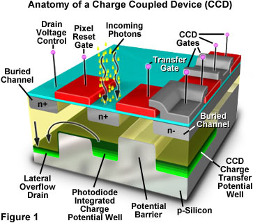
Charge-coupled devices (CCDs) are silicon-based integrated circuits consisting of a dense matrix of photodiodes that operate by converting light energy in the form of photons into an electronic charge. Electrons generated by the interaction of photons with silicon atoms are stored in a potential well and can subsequently be transferred across the chip through registers and output to an amplifier. The schematic diagram illustrated in Figure 1 shows various components that comprise the anatomy of a typical CCD.
Fabricated on silicon wafers much like integrated circuits, CCDs are processed in a series of complex photolithographic steps that involve etching, ion implantation, thin film deposition, metallization, and passivation to define various functions within the device. The silicon substrate is electrically doped to form p-type silicon, a material in which the main carriers are positively charged electron holes. Multiple dies, each capable of yielding a working device, are fabricated on each wafer before being cut with a diamond saw, tested, and packaged into a ceramic or polymer casing with a glass or quartz window through which light can pass to illuminate the photodiode array on the CCD surface.
When a ultraviolet, visible, or infrared photon strikes a silicon atom resting in or near a CCD photodiode, it will usually produce a free electron and a "hole" created by the temporary absence of the electron in the silicon crystalline lattice. The free electron is then collected in a potential well (located deep within the silicon in an area known as the depletion layer), while the hole is forced away from the well and eventually is displaced into the silicon substrate. Individual photodiodes are isolated electrically from their neighbors by a channel stop, which is formed by diffusing boron ions through a mask into the p-type silicon substrate.
Contributing Authors
Matthew J. Parry-Hill and Michael W. Davidson - National High Magnetic Field Laboratory, 1800 East Paul Dirac Dr., The Florida State University, Tallahassee, Florida, 32310.
BACK TO DIGITAL IMAGING IN OPTICAL MICROSCOPY