Electronic Imaging Detectors
Over the past several years, the rapidly growing field of fluorescence microscopy has evolved from a dependence on traditional photomicrography using emulsion-based film to one in which electronic images are the output of choice. The imaging device is one of the most critical components in fluorescence microscopy because it determines at what level specimen fluorescence may be detected, the relevant structures resolved, and/or the dynamics of a process visualized and recorded.
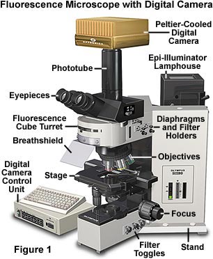
The range of light detection methods and the wide variety of imaging devices currently available to the microscopist make the selection process difficult and often confusing. This discussion is intended to aid in understanding the basics of light detection and to provide a guide for selecting a suitable detector for specific applications in fluorescence microscopy. Illustrated in Figure 1 is an epi-fluorescence microscope equipped with a state-of-the-art megapixel digital imaging camera system with Peltier cooling designed to image specimens over a wide exposure range in 24-bit color at low light levels. Detectors of this type as well as other alternatives are reviewed in the following paragraphs.
Detector Characterization Parameters
Electronic imaging sensor performance may be described by a number of variables including: spectral sensitivity, quantum efficiency, spatial resolution, uniformity, the signal/noise ratio, dynamic range, and response speed. Each of these specifications is discussed in detail in our section reviewing Concepts in Digital Imaging Technology, but a brief description is included here for convenience. Spectral sensitivity refers to the detector signal as a function of the wavelength of the incident light. This parameter is often expressed in terms of the quantum efficiency (QE), a measure of the detector's ability to produce an electronic charge from the percentage of incident photons that are detected. The limiting spatial resolution is commonly determined from the minimum separation required for discrimination between two high contrast objects, for instance, white points or lines on a black background. Contrast is an important factor in resolution because high contrast objects (e.g. black and white lines) are more readily resolved than low contrast objects (e.g. adjacent gray lines).
More informative measures of the spatial resolution of an electronic detector are the modulation transfer function (MTF) and the contrast transfer function (CTF), both of which demonstrate the magnitude of the detector response as a function of spatial frequency. The CTF is determined from the detector response to a series of black and white bars that become progressively narrower and closer together. Each pair of bars is essentially a square wave with 100 percent contrast. The MTF is an expression describing the reduction in contrast of a sinusoidal signal (60% contrast sine waves) as a function of spatial frequency. The limiting resolution of an electronic detector is the smallest target size that is detectable above the noise threshold, a concept that is often referred to as the frequency of limiting resolution, which is the spatial frequency for which the MTF falls to a value of 3 percent, corresponding to the limit of visible detection.
The uniformity of electronic detectors encompasses several variables: gain variations across the sensor, regional differences both in noise and sampling efficiency (often termed shading), and spatial variation in the efficiency of light collection or transmission. Electronic detectors are often compared by their signal/noise ratio (designated S/N), a measure of the variation of a signal that indicates the confidence with which the magnitude of the signal can be estimated. Visible light has an inherent noise component arising from the stochastic nature of the photon flux, which is equal to the square root of the signal. Noise also derives from a variety of other sources such as the output amplifier (read noise), and in electronic devices can often be reduced by lowering the operating temperature. Noise arising in electronic devices in the absence of light is termed dark current or dark noise, which is thermally sensitive, increasing as a function of the detector temperature.
Intrascene dynamic range is derived from the maximum and minimum intensities that can be simultaneously detected in the same field of view. Interscene dynamic range represents the range of intensities that can be accommodated when detector gain, integration time, lens aperture, or other variables are adjusted for differing fields of view. The terms dynamic range and signal/noise should not be confused. Dynamic range is often calculated as the maximum signal that can be accumulated divided by the noise associated with reading that signal. The response speed of an electronic detector is described by its lag, representing the fraction of the previous image that carries over into the next one after a prescribed time interval has elapsed.
Electronic Detection of Light
Two examples of commonly used light detectors lacking spatial discrimination are the photomultiplier tube and the photodiode (illustrated in Figure 2). Both devices employ a photosensitive surface that captures incident photons and generates electronic charges that are sensed and amplified. Photomultiplier tubes (PMTs) are widely used in confocal microscopes and high-end automatic exposure bodies for film cameras as well as in spectrometers. These devices respond when photons impinge on a photocathode and liberate electrons that are accelerated toward an electron multiplier composed of a series of curved plates, known as dynodes.
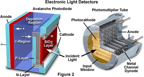
Light entering the input window of a PMT strikes the photocathode, which utilizes the energy of the incident photons to release electrons with a peak quantum efficiency that has recently been improved to about 40 percent (see the GaAsP curve in Figure 3). The photocathode active area can range in size from a few millimeters to a half meter in diameter, depending upon the application.
| Interactive Tutorial | |||||||||||
|
|||||||||||
The output from the metal channel dynode chain is a current proportional to the number of photons striking the photocathode and to the voltage drops along the dynode channel. Spectral sensitivity depends on the chemical composition of the photocathode; the best devices often incorporate gallium-arsenide and are sensitive to ultraviolet, visible, and infrared light in the wavelength range from 300 to 850 nanometers (Figure 3). PMT photocathodes are not uniformly sensitive and typically the photons are spread over the entire entrance window rather than concentrating into one region. Because PMTs do not store charge and respond to changes in input light fluxes within a few nanoseconds, they can be used for the detection and recording of extremely fast events. These devices typically generate low noise values (and dark current) resulting in a huge dynamic range over which electrical current output still accurately reflects the photon flux. The large gain exhibited by these devices is obtained without sacrificing bandwidth, which can range from 100 to 1500 MHz with a very high signal/noise ratio in scientific grade PMTs.
The spectral sensitivity curves for three electronic detectors illustrating quantum efficiency as a function of the illumination wavelength is presented in Figure 3. Two of the curves (the lower curves in Figure 3) were generated with PMTs having photocathode compositions utilizing either gallium-arsenide-phosphide (Ga-AS-P) or gallium-arsenide (Ga-As) alloys, while the third curve represents the response of a silicon photodiode with a ultraviolet-transparent window.
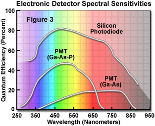
Silicon photodiodes also respond rapidly to light by the generation of a current, but they do so without the huge gain that accompanies electron multiplication by the PMT. Photodiodes have a relatively flat response over the entire visible spectrum (Figure 3) with high quantum efficiency that ranges from 80 to 90 percent. Uniformity of the photosensitive surface is excellent and the dynamic range and response speed of these devices are among the highest of any light detector. However, silicon diodes produce a considerable amount of noise, (much of it thermal) resulting in relatively poor signal-to-noise under photon-limited conditions, such as are common in fluorescence microscopy. Photodiodes that incorporate limited gain have been developed (avalanche photodiodes, illustrated in Figure 2) and been utilized in some confocal and wide-field fluorescence microscopes. Although they have up to 300-fold gain, they exhibit significant dark noise even when cooled to 0� C.
| Interactive Tutorial | |||||||||||
|
|||||||||||
Area Detectors
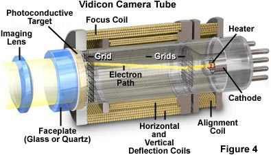
These devices are generally divided into two categories: tube-type and solid state detectors. The vidicon tube camera (illustrated in Figure 4) is a tube-type detector in which the photosensitive surface is "read out" by a scanning electron beam. In vidicons, the photosensitive surface stores charge rather than liberating electrons as in a photocathode. Photons captured by the photosensor alter its electrical resistance at their site of impact, and the current of the scanning beam flows more readily through these sites generating a signal. Because vidicon tube sensors have been largely supplanted by modern solid-state detectors and are of interest only due to historical significance, they will not be considered in any further detail.
Solid-state detectors consist of a dense matrix of photodiodes incorporating charge storage regions. Several variations on the basic concept are commercially available including the popular charge-coupled device (CCD), the charge-injection device (CID), and the complementary-metal-oxide-semiconductor detector (CMOS). In each of these detectors, a silicon diode photosensor (often denoted a pixel) is coupled to a charge storage region that is, in turn, connected to an amplifier that reads out the quantity of accumulated charge. In the CID and CMOS detectors, each individual photosensor has an amplifier associated with it and the combined signal from a row of amplifiers is output in parallel. Although techniques for charge storage by silicon photodetectors were known for many years before the development of the CCD, a suitable mechanism for the systematic read out of this stored charge needed to be devised before the device became a reality. In a CCD, there is typically only one amplifier at the corner of the entire array, and the stored charge is sequentially transferred through the parallel registers to a linear serial register and then to an output node adjacent to the read-out amplifier.
Because the CCD is presently the most widely used detector for fluorescence microscopy, we will consider its performance in more detail. Distinctions will be made, where appropriate, between the two classes of CCD cameras: consumer-grade and scientific-grade. It is important to point out that although all electronic detectors are analog devices that generate electrical currents or charges, cameras with an internal digitizer have recently been denoted digital cameras because they do not have an analog signal output.
Some CCD cameras used in scientific applications are operated at room temperature while others are cooled to reduce dark current (a 20�C decrease in temperature reduces the dark current of the CCD ten-fold). Because the charge storage wells do not fill with thermally-generated dark noise during the integration period, longer exposures are possible. Cooled cameras for scientific use are often designated slow-scan because their frame rate is less than that of a standard video camera.
A video-rate camera reads the stored charge and outputs a video field every 16.7 milliseconds to conform to the recommended standards (denoted RS-170 or RS-330) in which 30 video frames are produced per second with each frame consisting of two interlaced fields (the European standard format requires 50 fields per second with a field every 20 milliseconds). Video exploits the lag in our visual system by generating images at a rate faster than the critical flicker frequency, the video refresh frequency in which flicker is no longer perceived by the human eye. Each video field, containing 50 percent of the information in an entire frame, is obtained in sequence with the result that there is a 16.7 millisecond time difference between successive odd or even scan lines in the complete image. If the output of a video-rate camera is stopped and light is allowed to fall on the CCD for a prolonged period, the first two video fields produced contain all of the information accumulated during the integration period.
Interlacing of two video fields to produce a complete video frame was a clever solution to the engineering problem resulting from the bandwidth limitations of the electronics and signal transmission and reception components available at the time of the development of television. Now much higher frequency amplifiers and associated electronics permit the production, storage, and subsequent display at frame rates of up to 1000/second without the need to interlace scan lines. Such progressive-scan cameras produce a continuous scan from the top to the bottom of the image. This does not mean that the top lines were obtained before the bottom ones; rather, the devices first integrate the photon flux over the entire sensor and then rapidly displace the accumulated charge to a charge storage and transfer region that is protected from further illumination.
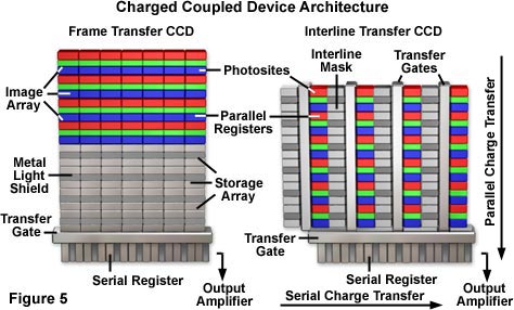
Two CCD designs are commonly used to achieve such rapid transfers: the interline-transfer CCD and the frame-transfer CCD, which are diagrammatically illustrated in Figure 5. The interline-transfer CCD incorporates charge transfer channels (termed "interline masks" in Figure 5) immediately adjacent to each photodiode so that the accumulated charge can be efficiently and rapidly shifted into the channels after image acquisition has been completed. Interline-transfer CCDs can be electronically shuttered by altering the voltages at the photodiode so that the generated charges are injected into the substrate rather than shifted to the transfer channels. These devices also include an electron "drain" to prevent blooming and are usually equipped with microlens arrays to increase the photodiode fill factor and quantum efficiency.
The frame-transfer CCD uses a two-part sensor in which one-half of the parallel array is used as a storage region and is protected from light by a light-tight mask. Incoming photons are allowed to fall on the uncovered portion of the array and the accumulated charge is then rapidly shifted into the masked storage region for charge transfer to the serial output register. While the signal is being integrated on the light-sensitive portion of the sensor, the stored charge is read out. A disadvantage of this architecture is charge smearing during the transfer from the light-sensitive to the masked regions of the CCD, but this can often be compensated.
| Interactive Tutorial | |||||||||||
|
|||||||||||
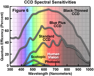
The spectral sensitivity of the CCD differs from that of a simple silicon photodiode detector because the CCD surface has channels used for charge transfer that are shielded by polysilicon gate electrodes. These structures absorb the shorter wavelengths and reduce the blue sensitivity of the device. A typical spectral sensitivity curve for a consumer or scientific-grade CCD is illustrated in Figure 6 (Standard CCD) where it should be noted that the peak quantum efficiency of 40 percent is markedly below that of a individual silicon photodiode. Recently, the transparency of the channels has been increased with substantial improvement in blue-green sensitivity of some scientific-grade CCDs (Blue Plus curve in Figure 6). The losses due to the channels are completely eliminated in the back-illuminated CCD. In this design, light falls onto the back of the CCD in a region that has been thinned by etching until it is transparent (a thickness corresponding to about 10-15 microns). The resultant spectral sensitivity curve, also shown in Figure 6 (Back-Thinned CCD), illustrates the high quantum efficiency that can be realized with this configuration. However, back-thinning results in a delicate, relatively expensive sensor that, to date, has only been employed in high-end scientific-grade CCD cameras.
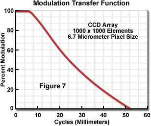
The resolution of a CCD is a function of the number of photodiodes and their size relative to the projected image. CCD arrays of 1000 x 1000 sensors are now commonplace in scientific-grade video cameras. The trend in consumer and scientific-grade CCD manufacture is for the sensor size to decrease, and cameras with photodiodes as small as 4 x 4 microns are currently available in the consumer market. A typical MTF curve for a CCD camera with 6.7-micron pixels is shown in Figure 7. The spatial frequency of 60-percent contrast sine waves projected onto the sensor surface is plotted on the abscissa and the resultant modulation percentage on the ordinate. The limiting resolution is normally defined as the 3 percent modulation level.
Adequate resolution of an object can only be achieved if at least two samples are made for each resolvable unit (many investigators prefer three samples per resolvable unit to ensure sufficient sampling). In the case of the epi-fluorescence microscope, the resolvable unit from the Abbe diffraction limit at a wavelength of 550 nanometers using a 1.4 numerical aperture lens is 0.21 microns. If a 100x objective is employed, the projected size of a diffraction-limited spot on the face of the CCD would be 21 microns. A sensor size of 10.5 x 10.5 microns would just allow the optical and electronic resolution to be matched, with a 7 x 7 micron sensor size preferred. Although small sensors in a CCD improve spatial resolution, they also limit the dynamic range of the device. Table 1 provides suggested sensor pixel size for commonly used objectives in fluorescence microscopy.
Pixel Size Requirements for Maximum Optical Resolution
in Fluorescence Microscopy
|
||||||||||||||||||||||||||||||||||||||||||||||
Table 1
The charge storage capacity of a CCD is proportional to the size of the individual photodiode, such that the maximum number of electrons stored is about 1000 times the cross sectional area of each photodiode. Thus, a CCD with 7 x 7 micron photodiodes should have a maximum charge storage capacity (a full-well capacity) of 49,000 electrons or holes. A hole is the region of the silicon from which the electron came and constitutes an equally valid and usable measure of detected photons. The term "electrons" will be used predominantly throughout this discussion even though many CCDs read out the number of holes generated rather than electrons. Because CCDs do not have inherent gain, one electron-hole pair is accumulated for each detected photon. The dynamic range of a CCD is typically defined as the full-well capacity divided by the camera noise. The camera noise is the sum, in quadrature, of the dark and read-out noise. Recent improvements in CCD design have greatly diminished dark charge to negligible levels and reduced read-out noise to about 10 electrons per pixel. Even room temperature cameras may have such a low dark signal that it can be ignored for integration periods of 10 seconds or less. Cooling further reduces the dark signal and permits much longer integration periods, up to several hours, without significant dark charge accumulation. Thus, the dynamic range of a 49,000 electron full-well capacity CCD with 10 electrons of read-out noise and negligible dark noise is about 4900, requiring a 12-bit analog-to-digital conversion, or 4,096 gray-level resolution, to fully utilize the image sensor dynamic range.
A CCD with a 49,000 electron full-well capacity has a maximum achievable signal/noise of about 220 (the square root of 49,000). Of course, camera noise would add, in quadrature, to the photon statistical noise and reduce the maximum signal-to-noise below this value. A simple estimate of the signal-to-noise of any homogeneous region in an image may be made from the average intensity of the region of interest divided by the standard deviation of the intensities of that region.
Cameras for consumer use often have a rectangular format CCD with an aspect ratio of 4:3. That means that the height of the image will be 3/4 of the width to conform with video standards based on our landscape view of the world. Indeed, the newest generation of consumer-grade products designed for HDTV employ a 16:9 aspect ratio. Scientific imaging, on the other hand, is best conducted with a square image made up of square pixels as they are better suited to digital image processing.
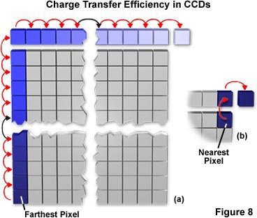
CCD sensor uniformity is generally very good, with less than 10 percent variation in gain between photodiodes. However, shading may be introduced into the image from a CCD camera because of inefficiencies in charge transfer. The operation of a CCD requires that each packet of charge underlying a photodiode be transferred to the read-out amplifier. This transfer is accomplished by a series of parallel and serial shifts that displace rows of charge along the chip toward a single corner containing the read-out amplifier. If the read-out amplifier is in the upper right-hand corner of a 1000 x 1000 sensor CCD, the charge from the photosensor nearest to that corner will have to be shifted only once upward into the serial shift register (a parallel shift) and once rightward (a serial shift) to reach the amplifier. On the other hand, the charge from the photodiode in the lower left hand corner will have to be shifted upward 1000 times and rightward 1000 times to be read out. If the transfer efficiency is 99.9 percent for each shift, only 13.5 percent of the charge accumulated by the lower left photodiode would remain after the requisite 2000 shifts. This charge loss would make the lower left corner much darker than the upper right and would also tend to blur or smear that region of the image because of spillover by charges from adjacent photodiodes. The concept is illustrated schematically in Figure 8 using blue colored pixels to represent integrated charge density. The pixel in the lower left hand corner of the CCD (farthest pixel - dark blue) is shown slowly losing color intensity as the charge is transferred first in parallel to the serial shift register, then serially to the output node. A pixel closer to the node (the upper right-hand "nearest" pixel) is also illustrated in dark blue and undergoes only a two-step jump to yield an accumulated charge transfer efficiency of 99.8 percent at the output node.
Slow-scan CCD cameras increase charge transfer efficiency by cooling the CCD and slowing the transfer rate. The high speed charge transfer required in video-rate CCD cameras necessitates a different strategy. In these cameras, the read-out amplifier gain is adjusted to compensate for the charge lost from each row by sampling extra pixels outside of the image area. The additional gain required for the lower rows inevitably increases the noise in the highly corrected regions of the sensor.
Some control over the read-out rate as well as the size of the pixel that constitutes a sensor is permitted by slow-scan CCD cameras. Video-rate CCD cameras are simpler and do not allow such control. Slowing the read-out usually reduces the amplifier noise associated with reading the charge, a beneficial situation when the photon flux is very low and the signal can be produced relatively slowly (in a second or two rather than in 33 milliseconds). Scientific-grade CCD cameras usually offer two or more read-out rates so that speed may be traded off against noise.
The size of a pixel in a scientific-grade CCD may be increased by binning, a process in which the charge from a cluster of adjacent photodiodes is pooled and treated as if it came from a larger detector. In binning, several shifts of charge to the serial register and output node storage regions occur before read out. The extent of binning depends on how many shifts occur before the stored charge is read, with the only limitation being the charge storage capacity of the serial register (usually twice that of a single photodiode) or of the output node (usually three times that of a photodiode). The maximum charge storage capacity of the serial register and output node are not a concern in most fluorescence microscopy applications because binning is employed when light levels are very low and few photons are detected. Binning enables the investigator to trade spatial resolution for sensitivity.
| Interactive Tutorial | |||||||||||
|
|||||||||||
There are a variety of scientific CCDs available on the market that feature a wide range of array and individual pixel sizes. Several of the most popular CCDs found in digital imaging cameras used in microscopy are listed in Table 2. Currently, the most popular CCD is the Sony ICX205AK interline-transfer progressive scan chip that supports a high frame readout rate of 30 frames/second. This CCD has a 1360 x 1024 active pixel array producing an 8-millimeter image size using 4.65 x 4.65 micron square pixels. The chip also features high sensitivity, low dark current, low smear, excellent antiblooming characteristics, and a continuous variable speed shutter.
CCD Specifications
|
||||||||||||||||||||||||||||||||||||||||||||||||||
Table 2
Slow-scan CCD cameras also allow region-of-interest read-out. This means that a selected portion of the image can be displayed and the remainder of the accumulated charge discarded. The framing rate generally increases with reduction in the size of the detected area. For example, a CCD with a sensor size of 1000 x 1000 and an output rate of ten frames/second can produce 100 frames/second if the read-out region is reduced to 100 x 100 diodes. By trading off field-of-view and framing rate, an investigator can adjust to a far wider range of experimental circumstances than would be possible with a fixed framing rate video camera.
Low-Light-Level Imaging of Fluorescence
Because of the problems of photodestruction of fluorochromes in the presence of oxygen ("photobleaching") and limitations on the numbers of fluorochromes that can be involved a single region, a variety of sensitive electronic detectors are used in fluorescence microscopy. Only about 5-10 percent of the emitted light from an excited fluorochrome is collected and transferred to the sensor in a typical epi-fluorescence microscope. There are two approaches to capturing as much of this limited light flux as possible: integration by a slow-scan CCD, as previously described, or image intensification and capture on a video-rate or progressive-scan CCD camera. The general finding is that a cooled, slow-scan CCD camera always produces a higher signal-to-noise than an intensified CCD, provided sufficient integration time is available.
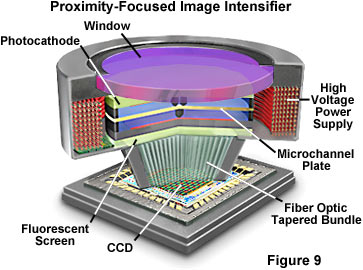
Image intensifiers (see the examples in Figures 9 through 11) were developed for military use to enhance our night vision. They have an input photocathode followed by a micro-channel plate electron multiplier and a phosphorescent output screen. The photocathode in the latest generation of these devices, while similar to that in photomultiplier tubes, has a higher quantum efficiency (up to 50 percent) in the blue-green end of the spectrum. The gain of the micro-channel plate is adjustable over a wide range with a typical maximum of about 80,000 (a detected photon at the input leads to a pulse of 80,000 photons from the phosphor screen). The phosphor matches the spectral sensitivity of the eye and is often not ideal for a CCD. Resolution of an intensified CCD depends on both the intensifier and the CCD, but is usually limited by the intensifier microchannel plate geometry to about 75 percent of that of the CCD alone. The latest generation of image intensifiers (denoted blue-plus Gen III or sometimes Gen IV; Figure 9) employ smaller microchannels (6 micron diameter) and better packing geometry than in previous models with a resultant substantial increase in resolution and elimination of the chicken-wire fixed-pattern noise that plagued earlier devices.
Image intensifiers have a reduced intrascene dynamic range compared to a slow-scan CCD camera and it is difficult to obtain more than a 256-fold intensity range (8 bits) from an intensified CCD camera. Intensifier gain may be rapidly and reproducibly changed to accommodate variations in scene brightness, thereby increasing the interscene dynamic range. Indeed, since image intensifiers can be rapidly gated (turned off or on in a few nanoseconds), relatively bright objects can be visualized by a reduction in the "on" time. A gated, variable gain intensified CCD camera is commercially available with a 12 order of magnitude dynamic range. Gated, intensified CCD cameras are required for most time-resolved fluorescence microscopy applications because the detector must be turned on and off in nanoseconds or its gain rapidly modulated in synchrony with the light source.
Thermal noise from the photocathode as well as electron multiplication noise from the microchannel plate reduce the signal-to-noise in an intensified CCD camera to below that of a slow-scan CCD. The contribution of these components to the noise created by the statistical nature of the photon flux depends on the gain of the device and the temperature of the photocathode. Generally, a reduction of the gain of the intensification stage is employed to limit the noise although intensified CCD cameras are available with a cooled photocathode.
Intensified CCD cameras have a very fast response limited by the time constant of the output phosphor and often the CCD camera read out is the slowest step in image acquisition. Because of the low light fluxes emanating from the fluorochromes bound to or within living cells, intensified CCD cameras are frequently employed to study dynamic events and for ratio imaging of ion-sensitive fluorochromes. The simultaneous or near-simultaneous acquisition of two images at different excitation or emission wavelengths is required for ratio imaging and intensified CCD cameras have the requisite speed and sensitivity.
| Interactive Tutorial | |||||||||||
|
|||||||||||
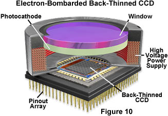
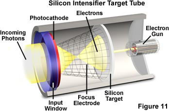
A hybrid of the image intensifier and the CCD camera is the recently introduced, electron-bombarded CCD (EBCCD; Figure 10). In this device, photons are detected by a photocathode similar to that in an image intensifier. The released electrons are accelerated across a gap and impact on the backside of a CCD. These energetic electrons generate multiple charges in the CCD resulting in a modest gain of a few hundred. The advantages of this device over a cooled, slow-scan CCD are the additional gain and accompanying speed; the main disadvantages are the lower quantum efficiency of the photocathode and diminished dynamic range. Compared to an intensified CCD, the electron bombarded CCD usually has higher spatial resolution and a better signal-to-noise at moderate light levels, but the limited gain adjustment range and modest low-light-level detection capability make the electron-bombarded CCD the solid-state equivalent of the outmoded SIT (silicon intensifier target; Figure 11) camera.
Electronic versus Visual Detection
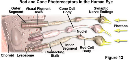
How does the human eye compare with electronic detectors? Figure 6 illustrates spectral sensitivity curves for the eye, corresponding to photopic and scotopic vision, arising from the cones and rods (Figure 12), respectively. Peak sensitivity is in the green (photopic at 555 nanometers and scotopic at 507 nanometers) with a maximum quantum efficiency of 3 percent for photopic vision and 10 percent for scotopic. Our spatial resolution is not uniform because the cones are not evenly distributed. The highest density occurs in the fovea where the distance between cones is about 1.5 microns, giving us a 5 to 6 micron limiting spatial resolution on the retina. Under achromatic (black and white) constant illumination conditions, visual intrascene dynamic range is only about 50-fold (6 bits). Our visual pigment, rhodopsin, exhibits little thermal noise, and the minimum detectable signal after dark adaptation is about 100 to 150 photons at the pupil or about 10 to 15 photons at the retina. The signal/noise for the eye at the visual detection limit is about 3:1. Lag is about 20 milliseconds at high light levels and about 100 milliseconds in dim illumination.
It is obvious that, compared to our eyes, a scientific-grade CCD camera has a broader spectral sensitivity, much higher quantum efficiency, greater integration capability, more uniformity, better intrascene dynamic range (more "bits"), comparable or higher signal/noise, but lower spatial resolution. When matched against our visual system, low-light-level cameras have a much wider spectral range, less lag and far greater sensitivity and resolution under photon-limited conditions.
Choosing the Appropriate Camera
No single detector will meet all requirements in fluorescence microscopy and the investigator is often forced into a compromise. In addition, the choice is made difficult because the slow-scan cameras are getting faster and the video-rate cameras are often cooled.
When time is the critical parameter, intensified cameras are often the only choice. If the event under investigation is rapid but can be precisely triggered, a slow-scan CCD operating in a burst or high-speed mode may be suitable. However, when the event is not readily predictable and the specimen must be monitored continuously at low incident light flux, the intensified CCD is the detector of choice. For this reason single molecule fluorescence studies have often employed intensified CCD cameras.
When time is available for image integration, a slow-scan CCD camera will usually outperform an intensified camera in all areas, in large part due to its higher quantum efficiency and lower noise. Cooling always improves camera performance although the difference may not be noticeable when the integration time is a few seconds or less and the digitization level is 10 to 12 bits or less. For applications involving digital deconvolution, the detector of choice is a cooled, scientific-grade, slow-scan camera capable of producing a high resolution, 14-bit to 16-bit image. However, some of the latest CCDs have such small pixels that the integration period must be limited to avoid saturation of the wells and, as a result, the dynamic range and peak signal-to-noise may be no better than those of an intensified CCD.
Two types of color CCD cameras are used for scientific applications: a single CCD with a wavelength selection filter or a three sensor (three chip) camera. Both use filters to produce red, green and blue versions of the field-of-view. The single sensor camera utilizes an adherent filter, filter wheel or liquid crystal tunable filter to acquire the red, green, and blue images. When a tunable filter or filter wheel are used, three images must be obtained in sequence. The three-sensor camera has a beam splitting prism and trim filters that enable each sensor to image the appropriate color and to acquire all three images simultaneously. Invariably, color cameras are less sensitive than their monochrome counterparts because of the additional beam-splitting and wavelength selection components. In some applications, particularly immunofluorescence, the loss of sensitivity is offset by being able to capture multiple wavelengths simultaneously. In addition, some color cameras achieve a higher resolution by employing a piezo-controlled translocation mechanism to offset the CCD slightly, thereby increasing the sampling frequency.
Recent improvements in the performance of CMOS cameras herald a potentially important future role for these devices in fluorescence microscopy. CMOS cameras have an amplifier and digitizer associated with each photodiode in an integrated on-chip format. The individual amplifiers associated with each pixel help reduce noise and distortion levels, but they also induce an artifact known as "fixed pattern noise" that arises from switching and sampling artifacts of individual pixel amplifiers. This is manifested by reproducible patterns of "mottle" behavior in the image generated by CMOS active pixel sensor devices. A great deal of research effort has been invested in solving this problem, and the residual level of noise has recently been dramatically reduced in CMOS sensors. The result is a cheap, compact, versatile detector combining the virtues of silicon detection without the problems of charge transfer. CMOS sensors allow gain manipulation of individual photodiodes, region-of-interest read-out, high speed sampling, electronic shuttering and exposure control. They have extraordinary dynamic range as well as an ideal format for the computer interface. It is likely that they will replace CCD cameras in a number of scientific applications in the near future.
Contributing Authors
Kenneth R. Spring - Scientific Consultant, Lusby, Maryland, 20657.
Michael W. Davidson - National High Magnetic Field Laboratory, 1800 East Paul Dirac Dr., The Florida State University, Tallahassee, Florida, 32310.
BACK TO DIGITAL IMAGING IN OPTICAL MICROSCOPY
BACK TO FLUORESCENCE MICROSCOPY
