
Introduction to Digital Photomicrography
Over the past decade, the quality of digital electronic cameras available for optical microscopy has greatly improved to the point that these devices are now overtaking film cameras in popularity and sales. Electronic cameras operate by capturing the image projected directly onto an electron tube or a solid state detector without the use of film.
A primary consideration in choosing a digital camera over film is whether the electronic imaging device is of adequate field size and spatial resolution to record the entire viewfield at the optical resolution of the microscope system. In recent years, the amount of information capable of being captured and stored by the best digital cameras is approaching (but still short of) the resolution available with traditional 35 millimeter film.
Digital images offer many opportunities for computer-controlled quantitative analysis, image manipulation, and digital enhancement as well as the advantage of permanence of digital storage. The highest quality digital cameras can cost many thousands of dollars, so the selection of an electronic camera for photomicrography must be preceded by careful consideration of its proposed use. New developments in microscopic optical systems, electronics, and computer technology have led to an expanded interest in the microscope as an investigative tool in the biological sciences, particularly in the fields of cell biology, neurobiology, and medicine. Industrial microscopy applications are also on the rise, with reflected light microscopes being increasingly employed in semiconductor fabrication, nanotechnology, and in metallography of new materials. These new developments have lured a battery of research scientists unfamiliar with classical photomicrography techniques, but well-versed in the use of computers and associated peripherials.
The specific microscopy application and its requirements must be carefully considered before making a commitment to a particular imaging device or system. This includes whether fixed or live specimens will be examined, and if absorbing or fluroescing dyes are to be used, whether imaging in grayscale or true color will be required. Contrast-enhancing techniques such as polarized light, differential interference contrast, phase contrast, and Hoffman modulation contrast present unique situations that should be reviewed when selecting a camera system. A camera's sensitivity to low light levels is a primary consideration for many of the contrast-enhancing techniques and is of critical concern in fluorescence photomicrography.
Resolution requirements should also be evaluated when choosing a digital camera. Routine inspection and recording of images during semiconductor fabrication does not require the same level of resolution as single-molecule events in fluorescence photomicrography of living cells and tissues. The microscope magnification range necessary for experiments will also dictate the level of resolution required to record satisfactory images. If the camera is to be used to capture full-motion video and/or time-lapse cinemicrography, then the interface and video feed rate into a computer or video cassette recorder must also be considered.
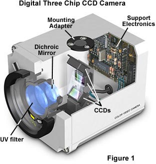
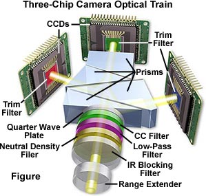
The two general types of electronic cameras available for microscopy are the tube cameras (Vidicon family) or charge-coupled device (CCD) cameras. Either type can be intensified for increased sensitivity to low light. The older silicon intensified tube (SIT) or newer intensified versions (ISIT) are useful for further intensification of tube cameras, while the ICCD is an intensified CCD camera. CCD cameras can also be cooled to increase sensitivity by giving a better signal to noise ratio. These kinds of cameras can be designed to respond to light levels undetectable by the human eye.
The criteria for selection of an electronic camera for microscopy include sensitivity of the camera, quantum efficiency, signal to noise ratio, spectral response, dynamic range capability, speed of image acquisition and readout, linearity or response, speed of response in relation to changes in light intensity, geometric accuracy, and ready adaptability to the microscope. A very important criterion for the newer digital CCD cameras is resolution. Current chips range from as few as 64 x 64 pixels up to 2048 x 2048 and above for very specialized applications, but larger arrays are continuously being introduced and, at some not-to-distant time, digital image resolution will rival that of film.
The purchaser must also decide whether or not the camera will operate at video rate (therefore being easily compatible with such accessories as video recorders or video printers). Tube cameras and CCD cameras are available for video rate operation. CCD cameras can also deliver slow acquisition or high-speed acquisition of images. Scientific, rather than commercial grade, CCD cameras are the variety most suitable for research.
CCD cameras are usually of small size. They have low distortion, no lag, and good linearity of response. These cameras are also more rugged and less susceptible to mishandling than tube cameras. Each pixel of the CCD camera serves as a well for charge storage of the incoming photons for subsequent readout. The depth of these wells relates to the quality of the response. Binning of adjacent pixels by joining them together into super pixels can be employed to speed readout in a slow-scan CCD camera.
An emerging technology that shows promise as the possible future of digital imaging is the active pixel sensor (APS) complementary metal oxide semiconductor (CMOS) camera on a chip. Mass production of CMOS devices is very economical and many facilities that are currently engaged in fabrication of microprocessors, memory, and support chips can be easily converted to produce CMOS optical sensors. Although CCD chips were responsible for the rapid development of video camcorders, the technology has remained trapped as a specialized process that requires custom tooling outside the mainstream of integrated circuit fabrication. Also, the CCD devices require a substantial amount of support circuitry and it is not unusual to find five to six circuit boards in a typical video camcorder.
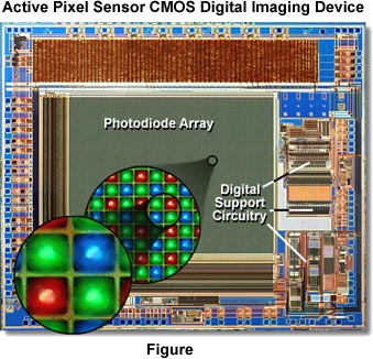
In the center of the APS CMOS integrated circuit is a large array of optical sensors that are individual photodiode elements covered with dyed filters and arranged in a periodic matrix. A photomicrograph of the entire die of a CMOS chip is illustrated in Figure xx. High magnification views of a single "pixel" element (Figure xx) reveal a group of four photodiodes containing filters based on the primary colors red, green, and blue. Each photodiode is masked by either a red, green, or blue filter in low-end chips, but higher resolution APS CMOS devices often use a teal (blue-green) filter in place of one of the green filters. Together, the four elements illustrated in Figure xx comprise the light-sensitive portion of the pixel. Two green filter masks are used because visible light has an average wavelength of 550 nanometers, which lies in the green color region. Each pixel element is controlled by a set of three transistors and an amplifier that work together to collect and organize distribution of optical information. The array is interconnected much like memory addresses and data busses on a DRAM chip so that the charge generated by photons striking each individual pixel can be accessed randomly to provide selective sampling of the CMOS sensor.
The individual amplifiers associated with each pixel help reduce noise and distortion levels, but they also induce an artifact known as fixed pattern noise that arises from small differences in the behavior of individual pixel amplifiers. This is manifested by reproducible patterns of speckle behavior in the image generated by CMOS active pixel sensor devices. A great deal of research effort has been invested in solving this problem, and the residual level of noise has been dramatically reduced in CMOS sensors. Another feature of CMOS active pixel sensors is the lack of column streaking due to pixel bloom when shift registers overflow. This problem is serious with the CCDs found in most video camcorders. Another phenomenon, known as smear, which is caused by charge transfer in CCD chips under illumination, is also absent in CMOS active pixel sensor devices.
Assisting the CMOS device is a coprocessor that is matched to the APS CMOS to optimize the handling of image data. Incorporated into the coprocessor is a proprietary digital video processor engine that is capable of performing automatic exposure and gain control, white balance, color matrixing, gamma correction, and aperture control. The CMOS sensor and coprocessor perform the key functions of image capture, digital video image processing, video compression, and interfacing to the main computer microprocessor. The primary concerns with CMOS technology are the rather low quality, noisy images that are obtained with respect to similar CCD devices. These are due primarily to process variations that produce a slightly different response in each pixel, which appears in the image as snow. Another problem is that the total amount of chip area that is sensitive to light is less in CMOS devices, thus making them less sensitive to light. These problems will be overcome as process technology advances and it is very possible that CMOS devices will eclipse the CCD as the technology of choice in the very near future.
Short Takes
The quality of a photomicrograph, either digital or recorded on film, is dependent upon the quality of the microscopy. Film is a stern judge of how good the microscopy has been prior to capturing the image. It is essential that the microscope be configured using Köhler illumination, and that the field and condenser diaphragms are adjusted correctly and the condenser height is optimized. When properly adjusted, the microscope will yield images that have even illumination over the entire field of view and display the best compromise of contrast and resolution.
Contributing Authors
Mortimer Abramowitz - Olympus America, Inc., Two Corporate Center Drive., Melville, New York, 11747.
Michael W. Davidson - National High Magnetic Field Laboratory, 1800 East Paul Dirac Dr., The Florida State University, Tallahassee, Florida, 32310.