
Concepts in Digital Imaging Technology
Two Phase CCD Clocking
Charge transfer through CCD shift registers occurs after integration to relocate accumulated charge information to the sense amplifier, which is physically separated from the parallel pixel array. Several clocking schemes, including the two phase technique illustrated in Figure 1, are utilized to transfer charge from the collection gates to the output node.
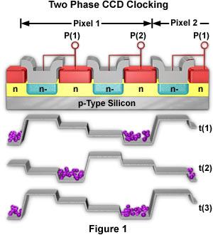
A two phase charge transfer CCD clocking scheme employs four gates for each pixel, with adjacent gates connected together as pairs. The two phase CCD scheme requires a more complex clocking arrangement than that described for the four phase and three phase CCD architectures. The shift register illustrated in Figure 1 includes one and a half pixel elements, for a total of six gates aligned along a common axis to form a column. Each gate pair is connected to an alternate clock line and one of the gates in each pair is designed with an increased n-type doping level beneath the gate. When voltage is applied to the gate pair, the gate having the increased doping level has a more positive potential, which increases the depth of the charge storage area and results in a "step" in the potential energy profile.
| Interactive Tutorial | |||||||||||
|
|||||||||||
The nature of electrostatic forces in the silicon substrate beneath the gates is determined by the voltage level applied to a particular gate by the clock input signal. High level voltages induce the formation of a potential "well" beneath the gate, whereas low level voltages form a potential barrier to electron movement. Clock lines are alternately pulsed, resulting in the charge packets (illustrated as purple "electrons" in Figure 1) being shifted along the CCD in a direction that is determined by the position of the extra doping. The requirement for only two clock phases reduces the complexity of the device, but at the expense of extra processing.
The initial state (at t(1) of the CCD illustrated in Figure 1) is with the combined gates at P(1) having a low-level voltage forming a pair of stepped potential barriers, with the potential higher in the region beneath the gate having the increased doping level. At the same time, the combined gates at P(2) have a high-level voltage and form stepped potential wells, in which the deepest well appears beneath the gate having a normal doping level (wells filled with purple spheres represent integrated charge or "electrons"). At t(2), to complete the short cycle, voltage levels are reversed with the gates at P(1) having the high-level voltages (and the potential wells) and the gates at P(2) having the low-level voltages.
Contributing Authors
Mortimer Abramowitz - Olympus America, Inc., Two Corporate Center Drive., Melville, New York, 11747.
Michael W. Davidson - National High Magnetic Field Laboratory, 1800 East Paul Dirac Dr., The Florida State University, Tallahassee, Florida, 32310.
BACK TO CONCEPTS IN DIGITAL IMAGING TECHNOLOGY