
Concepts in Digital Imaging Technology
CCD Scanning Formats
Charge-coupled device (CCD) digital imaging sensors are capable of acquiring images in one of three formats: point scanning, line scanning, and area scanning. Each of these formats has specific applications in digital photography and scanning of documents and images.
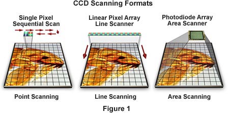
The simplest digital scanning technique utilizes a single pixel-cell detector to scan an image sequentially throughout a series of X and Y coordinates. CCD detectors of this type are relatively inexpensive and provide a uniform measurement from one scan site to another. The major disadvantage of this type of system is the repeated number of digital exposures necessary to compose an entire image and the mechanical complexity of the camera X-Y translation mechanism. Registration errors can also degrade images produced in this manner, although complex algorithms can often be employed to overcome this handicap.
A linear array of single-cell CCD detectors can be used to linearly scan along a single axis to produce a digital image, dramatically improving performance over that of the sequential scan format. Scanning takes place in a single direction where each line of information is captured, stored, and amplified before stepping to the next. This type of mechanism is commonly used in desktop flatbed scanners. In systems with colored filters placed over the photodiode elements, an image can be captured in a single pass, eliminating registration problems caused by three-pass systems. The size of the CCD scanning element is limited by a number of factors including wafer size, fabrication complexity, and mechanical restrictions on the stepper mechanism. In many cases, several linear CCD elements are positioned in series to increase the overall length of the scanning detector.
Linear CCD scanners (Figure 1) provide a higher rate of image acquisition when compared to single cell detectors, and they are also capable of producing high resolution images with less sophisticated scanning mechanics. Image resolution is restricted by pixel spacing and size, and scan times are usually on the order of seconds to minutes, making these devices largely unsuitable for camera applications.
The most sophisticated digital scanning technique (area scanning; see Figure 1) uses two-dimensional pixel array detectors, which allow an entire image to be captured with a single exposure. This method eliminates movement of the image sensor and the need for costly mechanical translation devices. Area scanners provide the fastest image acquisition frame rates with a high degree of registration accuracy between pixels, making them the ideal detection devices for digital cameras. Drawbacks include a limitation of resolution and a lower signal-to-noise performance when compared to the devices described above. Device cost is generally higher because of lower yields from the semiconductor fabrication techniques used to produce such complex chips.
Contributing Authors
Mortimer Abramowitz - Olympus America, Inc., Two Corporate Center Drive., Melville, New York, 11747.
Michael W. Davidson - National High Magnetic Field Laboratory, 1800 East Paul Dirac Dr., The Florida State University, Tallahassee, Florida, 32310.
BACK TO CONCEPTS IN DIGITAL IMAGING TECHNOLOGY