
Concepts in Digital Imaging Technology
Quantum Efficiency
The quantum efficiency of a charge-coupled device (CCD) is a property of the photovoltaic response defined as the number of electron-hole pairs created and successfully read out by the device for each incoming photon. This property is especially important for low-light imaging applications such as fluorescence microscopy where emission photon wavelengths are often in the 375-550 nanometer range and have a relatively high absorption coefficient in silicon. Standard CCDs, which are illuminated in the front of the device through the gate electrodes and oxide coatings, are more sensitive to green and red wavelengths in the region between 550 and 900 nanometers.
The spectral sensitivity of the CCD differs from that of a simple silicon photodiode detector because the CCD surface has channels used for charge transfer that are shielded by polysilicon gate electrodes, thin films of silicon dioxide, and a silicon nitride passivation layer. These structures, used to transfer the charge from the imaging area and to protect the CCD from humidity and electrostatic discharge, absorb the shorter wavelengths (450 nanometers and lower), reducing the blue sensitivity of the device. Polysilicon transmittance starts to decrease below 600 nanometers and the material becomes essentially opaque to photons at 400 nanometers, but absorption depends upon gate thickness and interference effects of light passing through thin films on the CCD surface. Interline-transfer CCDs have photodiodes that deviate from standard polysilicon gate structure, a factor that reduces interference effects and produces a more ideal and uniform spectral response. These devices are also usually equipped with vertical antibloom drains that produce a reduced response to longer wavelength photons. As photons above 700 nanometers penetrate deep into the silicon substrate close to the buried drain, they have a greater chance of liberating electrons that will diffuse into the drain and be instantly removed. Quantum efficiency is also dependent upon gate voltage, with lower voltages producing small depletion regions and visa versa.
Traditional film emulsions are hypersensitive to the blue region of the visible light spectrum, in contrast to the response displayed by CCDs, a feature that often results in color differences between images captured on film and those recorded with a CCD. As pixel geometry's grow smaller, the blue light absorption problem increases as the blue response of the sensor decreases rapidly with pixel size.
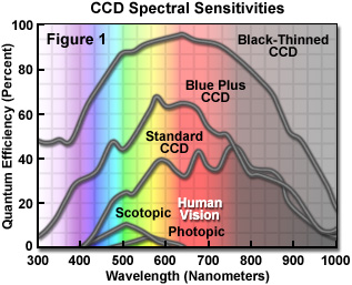
A typical spectral sensitivity curve for a standard CCD is illustrated in Figure 1 (Standard CCD) where it should be noted that the peak quantum efficiency of 40 percent is markedly below that of a individual silicon photodiode. Ripples in the spectrum occur because of interference effects from thin films on the CCD surface. Recently, transparency of the channels has been increased with substantial improvement in blue-green sensitivity of some scientific-grade CCDs (Blue Plus curve in Figure 1) through the use of pioneering gate materials and proprietary phosphor coatings. Coatings of this type (Lumogen) are deposited directly onto the array surface and emit light in the 500 to 580 nanometer region when excited by short wavelength (120 to 450 nanometer) high-energy ultraviolet and visible light. Phosphors embedded within the coating produce a secondary fluorescence that is emitted in all directions, with only those photons entering the array being absorbed to yield a quantum efficiency of approximately 15 to 20 percent. The coatings are transparent to visible light, so they do not affect photon absorption at wavelengths exceeding 450 nanometers, producing an apparent spectral response range of almost 1000 nanometers (120 to 1100 nanometers).
For comparison, Figure 1 also illustrates spectral sensitivity curves for the human eye, corresponding to photopic and scotopic vision, arising from the cones and rods, respectively. Peak sensitivity is in the green (photopic at 555 nanometers and scotopic at 507 nanometers) with a maximum quantum efficiency of 3 percent for photopic vision and 10 percent for scotopic. From this data it is obvious that compared to our eyes, a scientific-grade CCD camera has a broader spectral sensitivity with a much higher quantum efficiency.
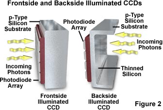
The losses due to gate channel structures are completely eliminated in the back-illuminated CCD. In this design, light falls onto the back of the CCD in a region that has been thinned by etching until it is transparent (a thickness corresponding to about 10-15 microns). The resultant spectral sensitivity curve, also shown in Figures 1 and 2 (Back-Thinned and Back-Illuminated CCD), illustrates the high quantum efficiency that can be realized with this configuration. However, back-thinning results in a delicate, relatively expensive sensor that, to date, has only been employed in high-end scientific-grade CCD cameras.
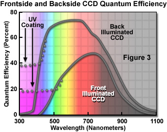
Anti-reflection coatings are used in back-thinned CCDs to increase quantum efficiency, but it is not possible to produce coatings that are effective across the entire visible range. Coatings that increase spectral response in the longer wavelengths often produce a corresponding decrease in absorption of lower wavelength photons, so research is ongoing to produce anti-reflection coatings that are effective across the entire visible light spectrum.
The photovoltaic effect, where light energy in the form of photons is converted into electronic potential, is dependent upon a wide spectrum of conditions. When visible and infrared photons in the 400 to 1100 nanometer range collide with a silicon atom positioned within the substrate of a CCD, electrons are excited from the valence band to the conduction band due to a reaction between the photons and silicon orbital electrons. A number of factors determine the amount of electronic charge generated by a quanta of light energy, including the absorption coefficient, photon recombination lifetime, diffusion length, and the chemical and physical nature of overlying materials on the CCD surface. The absorption coefficient of photons in silicon is wavelength dependent, with long-wavelength (greater than 800 nanometers) photons penetrating deeper into the silicon substrate than those having shorter wavelengths.
| Interactive Tutorial | |||||||||||
|
|||||||||||
In cases where the photon energy is greater than the band gap energy, an electron has a high probability of being excited into the conduction band, thus becoming mobile. This interaction is also known as the photoelectric effect, and is dependent upon a critical wavelength above which photons have insufficient energy to excite or promote an electron positioned in the valence band and produce an electron-hole pair. When photons exceed the critical wavelength (usually beyond 1100 nanometers), band gap energy is greater than the intrinsic photon energy, and photons pass completely through the silicon substrate. Table 1 lists the depth (in microns) at which 90 percent of incident photons are absorbed by a typical CCD.
Most of the photons with a wavelength between 450 and 700 nanometers are absorbed either in the depletion region or within the bulk material (silicon) of a CCD substrate. Those absorbed into the depletion region will have a quantum efficiency approaching 100 percent, whereas photons entering the substrate liberate electrons that experience a three-dimensional random walk and either recombine with holes or diffuse into the depletion region. For those electrons that have negligible diffusion lengths, the quantum efficiency is very low, but those with high diffusion lengths eventually reach a charge well.
Photon Absorption Depth in Silicon
|
||||||||||||||||||||||||||||||||||
Table 1
Most CCD arrays utilized in digital cameras designed for scientific applications are sealed within a protected environment to reduce artifacts, improve response, and prolong CCD life. Incoming photons often must pass through a glass or quartz window to reach the pixel array and enter the silicon substrate. Reflection losses at the window surface occur at all photon wavelengths, and transmittance of photons through glass (but not quartz) decreases dramatically for wavelengths below 400 nanometers. Scientific CCD sensors are designed for applications requiring high sensitivity and use quartz coatings to decrease reflection across all wavelengths.
Contributing Authors
Kenneth R. Spring - Scientific Consultant, Lusby, Maryland, 20657.
Michael W. Davidson - National High Magnetic Field Laboratory, 1800 East Paul Dirac Dr., The Florida State University, Tallahassee, Florida, 32310.
BACK TO CONCEPTS IN DIGITAL IMAGING TECHNOLOGY