
Concepts in Digital Imaging Technology
CCD Resolution for Optical Microscopy
The efficiency of capturing images generated by an optical microscope onto the pixel array of a charge-coupled device (CCD) is dependent upon several factors, ranging from the objective magnification and numerical aperture to the CCD array size and the dimensions of individual pixels within the array.
Photomicrography with traditional film cameras takes advantage of the high resolution capabilities of modern film emulsions to ensure that all information provided by the objective is accurately recorded in the grain structure of film images. As CCD technology evolves, pixel dimensions continue to decrease while array sizes simultaneously grow larger and more efficient. Many of the current digital imaging cameras designed for optical microscopy utilize the Sony ICX085AK progressive scan CCD image sensor that features a pixel array size of 1300 x 1030, or approximately 1.3 million pixels. This chip enjoys the advantage of interline charge transfer technology and has an active array aspect ratio of 5:4 with square pixel dimensions of 6.7 microns. Other properties that are responsible for the popularity of this CCD include high resolution and color reproductivity, high sensitivity, low dark current, low smear, and excellent anti-blooming characteristics.
The ultimate resolution of a CCD is a function of the number of photodiodes and their size relative to the image projected onto the surface by the microscope optics. CCD arrays vary in size from several hundred to thousands of pixels, as described in Table 1. Modern array sizes used in devices intended for scientific investigations range from 1000 x 1000 up to 4000 x 4000 sensor elements. The trend in consumer and scientific-grade CCD manufacture is for the sensor size to decrese, and digital cameras with photodiodes as small as 4 x 4 microns are currently available in the consumer market.
Adaquate resolution of a specimen imaged with the optical elements of a microscope can only be achieved if at least two samples are made for each resolvable unit, although many investigators prefer three samples per resolvable unit to ensure sufficient sampling. In diffraction limited optical instruments, such as the microscope, the Abbe limit of optical resolution at an average wavelength of 550 nanometers is 0.22 microns when using an objective lens having a numerical aperture of 1.4. In this case, a sensor size of 11 x 11 microns would be just large enough to allow the optical and electronic resolution to be matched, with a 7 x 7 micron sensor size preferred. Although small sensors in a CCD improve the spatial resolution, they also limit the dynamic range of the device.
CCD Specifications
|
||||||||||||||||||||||||||||||||||||||||||||||||||
Table 1
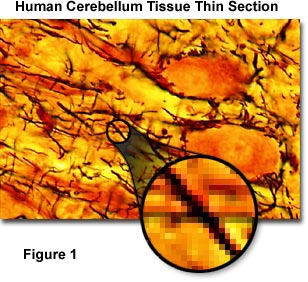
The photomicrograph in Figure 1 illustrates a thin section of human cerebellum brain tissue impregnated with a solution of silver nitrate, which stains selected portions of the neurons black. A gold-yellowish background color pervades the entire section, but this cast is an artifact of the method and not due to a counterstain. The image was captured digitally using an Olympus DP-11 digital camera operating in high resolution mode using a Nikon Eclipse E-600 microscope and a 40x fluorite objective having a numerical aperture of 0.75 with a 1x C-mount adapter lacking a projection lens. Assuming an average wavelength of 580 nanometers (green light), the resolution for this objective is 0.39 microns, which yields a projected size of 7.7 microns on the CCD surface. The DP-11 CCD is a progressive scan, interline transfer device having a Bayer RGB mosaic filter complement and a pixel size of 6.7 microns. Calculations (described below) of the minimum number of pixels required to capture the image at the maximum spatial resolution produced by the microscope optics indicate that a CCD array with 3.9 million pixels is required. DP-11 has an effective array of 2.4 million pixels arranged at 1784 (horizontal) x 1382 (vertical).
The wavelength spectrum of visible light used to create an image of a specimen is one of the determining factors in the performance of the microscope with respect to optical resolution. Shorter wavelengths (375-500 nanometers) are capable of resolving details to a greater degree than are the longer wavelengths (greater than 500 nanometers). The limits of spatial resolution are also dictated by the diffraction of light through the optical system, a term that is generally referred to as "diffraction limited" resolution. Investigators have derived several equations that have been used to express the relationship between numerical aperture, wavelength, and optical resolution:
|
R = |
(1) |
|
R = 0.61 |
(2) |
|
R = 1.22 |
(3) |
Where R is resolution (the smallest resolvable distance between two objects), NA equals numerical aperture, ![]() equals wavelength, NA(obj) equals the objective numerical aperture, and NA(Cond) is the condenser numerical aperture. Notice that equation (1) and (2) differ by the multiplication factor, which is 0.5 for equation (1) and 0.61 for equation (2). These equations are based upon a number of factors, including a variety of theoretical calculations made by optical physicists to account for the behavior of objectives and condensers, and should not be considered an absolute value of any one general physical law. The assumption is that two point light sources can be resolved (separately imaged) when the center of the Airy disk generated by one of the sources overlaps with the first order reflection in the diffraction pattern of the second Airy disk, a condition known as the Rayleigh Criterion. In some instances, such as confocal and fluorescence microscopy, the resolution may actually exceed the limits placed by any one of these three equations. Other factors, such as low specimen contrast and improper illumination may serve to lower resolution and, more often than not, the real-world maximum value of R (about 0.22 microns using a mid-spectrum wavelength of 580 nanometers) and a numerical aperture of 1.35 to 1.40 are not realized in practice.
equals wavelength, NA(obj) equals the objective numerical aperture, and NA(Cond) is the condenser numerical aperture. Notice that equation (1) and (2) differ by the multiplication factor, which is 0.5 for equation (1) and 0.61 for equation (2). These equations are based upon a number of factors, including a variety of theoretical calculations made by optical physicists to account for the behavior of objectives and condensers, and should not be considered an absolute value of any one general physical law. The assumption is that two point light sources can be resolved (separately imaged) when the center of the Airy disk generated by one of the sources overlaps with the first order reflection in the diffraction pattern of the second Airy disk, a condition known as the Rayleigh Criterion. In some instances, such as confocal and fluorescence microscopy, the resolution may actually exceed the limits placed by any one of these three equations. Other factors, such as low specimen contrast and improper illumination may serve to lower resolution and, more often than not, the real-world maximum value of R (about 0.22 microns using a mid-spectrum wavelength of 580 nanometers) and a numerical aperture of 1.35 to 1.40 are not realized in practice.
When the microscope is in perfect alignment and has the objectives appropriately matched with the substage condenser, then we can substitute the numerical aperture of the objective into equations (1) and (2), with the added result that equation (3) reduces to equation (2). An important concept to note is that magnification does not appear as a factor in any of these equations, because only numerical aperture and wavelength of the illuminating light determine specimen resolution. As we have mentioned (and can be seen in the equations) the wavelength of light is an important factor in the resolution of a microscope. Shorter wavelengths yield higher resolution (lower values for R) and visa versa. The greatest resolving power in optical microscopy is realized with near-ultraviolet light, the shortest effective imaging wavelength. Near-ultraviolet light is followed by blue, then green, and finally red light in the ability to resolve specimen detail. Under most circumstances, microscopists use white light generated by a tungsten-halogen bulb to illuminate the specimen. The visible light spectrum is centered at about 550 nanometers, the dominant wavelength for green light (our eyes are most sensitive to green light). It is this wavelength that was used to calculate resolution values in Table 2. The numerical aperture value is also important in these equations and higher numerical apertures will also produce higher resolution (see Table 2). The effect of the wavelength of light on resolution, at a fixed numerical aperture (0.95), is listed in Table 2.
Resolution versus Wavelength
|
||||||||||||||||||||
Table 2
In a system where the numerical aperture of the objective and condenser are matched and equal to a value of 0.95, and using a value of 580 nanometers (0.58 microns) for the average wavelength, the solution becomes:
The image size projected onto the surface of the CCD detector equals the optical resolution multiplied by the objective magnification:
The objective used in these calculations is a 40x plan apochromat having a numerical aperture of 0.95. Thus, the image size projected onto the CCD surface is:
To convert the image size projected onto the CCD surface (0.01221 millimeters) into line pairs per millimeter, we take the reciprocal of the projected size:
Line pairs per millimeter can be converted into equivalent TV lines by multiplying this quantity by the vertical CCD dimension (in this case, 6.4 millimeters) times a factor of 2:
The CCD maxiumum resolution can now be calculated by multiplying the number of TV lines by the CCD aspect ratio (5/4 or 1.25 for this example).
Finally, the minimum number of pixels required to match the optical resolution of the microscope can be calculated by multiplying the number of TV lines times the CCD maximum resolution.
Pixel Size Requirements for Optical Resolution
|
||||||||||||||||||||||||||||||||||||||||||||||||||||||||||||||||||||||||||||||||||||||||||||||||||||||||||
Table 3
Contributing Authors
Mortimer Abramowitz - Olympus America, Inc., Two Corporate Center Drive., Melville, New York, 11747.
Michael W. Davidson - National High Magnetic Field Laboratory, 1800 East Paul Dirac Dr., The Florida State University, Tallahassee, Florida, 32310.
BACK TO CONCEPTS IN DIGITAL IMAGING TECHNOLOGY