Concepts in Digital Imaging Technology
Frame-Transfer CCD Architecture
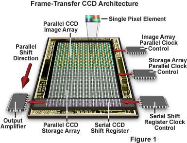
Frame-Transfer charged coupled image sensors have an architecture similar to that of full-frame CCDs. These devices have a parallel shift register that is divided into two separate and almost identical areas, termed the Image and Storage arrays.

The image array consists of a light-sensitive photodiode register, which acts as the image plane and collects incoming photons projected onto the CCD surface by the camera or microscope lenses. After image data has been collected and converted into electrical potential by the image array, the data is then quickly shifted in a parallel transfer to the storage array for readout by the serial shift register. Transfer time from the image-integrating array to the shielded storage array is dependent upon the pixel array sizes, but is typically on the order of 500 microseconds or less. The storage array is not light sensitive in most frame-transfer CCD designs, however some arrays are not equipped with an integral light shield. Arrays of the this design are capable of being operated in either full-frame or frame-transfer modes. With the use of a mechanical shutter, a frame-transfer CCD can be used to quickly capture two sequential images, a useful feature in fluorescence microscopy and other applications that require simultaneous acquisition of images generated at different emission and/or excitation wavelengths.
| Interactive Tutorial | |||||||||||
|
|||||||||||
As presented in Figure 1, the storage array is illustrated as a large area of gray-scale "pixels" that have been covered with an opaque metal mask or light shield to prevent any potential interaction with incoming photons. A miniature portion of the total image is contained in each pixel element, which consists of four photodiodes masked with red, green, and blue colored filters. The image presented in the upper right-hand corner of Figure 1 is an actual high-magnification photomicrograph of a single pixel element. Like the full-frame architecture, the frame-transfer CCD undergoes readout by shifting rows of image information in a parallel fashion, one row at a time, to the serial shift register. The serial register then sequentially shifts each row of image information to an output amplifier as a serial data stream. The entire process is repeated until all rows of image data are transferred off the chip, first to a signal output amplifier and then to an analog-to-digital signal converter integrated circuit. Reconstruction of the image in a digital format yields the final photograph or photomicrograph.
During the period in which the parallel storage array is being read, the image array is busy integrating charge for the next image frame. A major advantage of this architecture is the ability of the frame-transfer device to operate without a shutter or synchronized strobe, allowing for an increase in device speed and faster frame rates. Frame-transfer CCDs suffer from several drawbacks including image "smear", which occurs because integration and dump to the storage array occur simultaneously. Smear artifacts are limited to the time necessary for transfer of image integration data to the storage array. Frame-transfer devices are also more costly to produce because twice the silicon area is required to implement the architecture, resulting in lower image resolution and higher cost.
Contributing Authors
Mortimer Abramowitz - Olympus America, Inc., Two Corporate Center Drive., Melville, New York, 11747.
Michael W. Davidson - National High Magnetic Field Laboratory, 1800 East Paul Dirac Dr., The Florida State University, Tallahassee, Florida, 32310.
BACK TO CONCEPTS IN DIGITAL IMAGING TECHNOLOGY
