
Concepts in Digital Imaging Technology
Avalanche Photodiodes
An avalanche photodiode is a silicon-based semiconductor containing a pn junction consisting of a positively doped p region and a negatively doped n region sandwiching an area of neutral charge termed the depletion region. These diodes provide gain by the generation of electron-hole pairs from an energetic electron that creates an "avalanche" of electrons in the substrate.
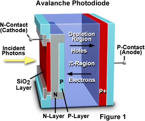
Presented in Figure 1 is an illustration of a typical avalanche photodiode. Photons entering the diode first pass through the silicon dioxide layer and then through the n and p layers before entering the depletion region where they excite free electrons and holes, which then migrate to the cathode and anode, respectively. When a semiconductor diode has a reverse bias (voltage) applied and the crystal junction between the p and n layers is illuminated, then a current will flow in proportion to the number of photons incident upon the junction.
| Interactive Tutorial | |||||||||||
|
|||||||||||
Avalanche diodes are very similar in design to the silicon p-i-n diode, however the depletion layer in an avalanche photodiode is relatively thin, resulting in a very steep localized electrical field across the narrow junction. In operation, very high reverse-bias voltages (up to 2500 volts) are applied across the device. As the bias voltage is increased, electrons generated in the p layer continue to increase in energy as they undergo multiple collisions with the crystalline silicon lattice. This "avalanche" of electrons eventually results in electron multiplication that is analogous to the process occurring in one of the dynodes of a photomultiplier tube.
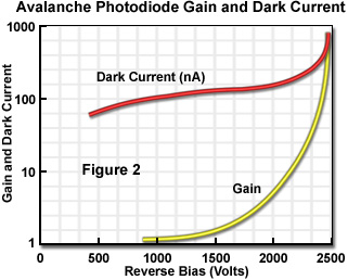
Avalanche photodiodes are capable of modest gain (500-1000), but exhibit substantial dark current, which increases markedly as the bias voltage is increased (see Figure 2). They are compact and immune to magnetic fields, require low currents, are difficult to overload, and have a high quantum efficiency that can reach 90 percent. Avalanche photodiodes are now being used in place of photomultiplier tubes for many low-light-level applications.
Contributing Authors
Kenneth R. Spring - Scientific Consultant, Lusby, Maryland, 20657.
Michael W. Davidson - National High Magnetic Field Laboratory, 1800 East Paul Dirac Dr., The Florida State University, Tallahassee, Florida, 32310.
BACK TO CONCEPTS IN DIGITAL IMAGING TECHNOLOGY