
Digital Imaging Techniques
Digital Image Acquisition
Digitizing the Output of an Analog Video Camera
The output from a majority of present-day video sensors and cameras, such as charge-coupled devices (CCDs) and vidicon tubes, is still in the analog form. With analog signals, the first stage in digital image processing systems is an electronic digitizer, the analog-to-digital (A/D) converter, or ADC, utilized to convert the analog output of the camera or sensor to a sequence of integer numerical values.
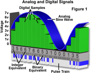
The analog-to-digital converter changes the incoming analog video signal stream into a series of integers conceptually structured as in a video frame. For example, the video frame may be divided into 640 equal-size boxes and vertically into 480 boxes (the number of effective video scan lines). Each horizontal video scan line is thus subdivided into 640 discrete units, each representing a time interval, or distance along the x-axis of the video image. Each box holds the integer number that specifies the amplitude of the video signal (image brightness) at that location. As a digital signal, a particular location is given by two integer numbers that denote its x and y coordinates, together with the integer that denotes the signal amplitude. Thus, a video frame is represented by an array of numbers that include the location of each box and the encoded value of the signal at that location.
The analog voltage must be sampled frequently enough in time (i.e., space along the horizontal scan line) and amplitude (or brightness) to produce a faithful numerical reproduction of the signal. Often the questions with what accuracy should the amplitude of the signal be converted and how frequently should samples be taken come up and are provided a good overview in A Guide to Selecting Electronic Cameras for Light-Microscope-Based Imaging.
Required Amplitude Resolution
An RS-170 video signal is composed of a picture signal and associated timing (or synchronization) signals. The audio-to-digital converter needs to convert only the picture signal into numerical values while the synchronization signals are detected, stripped, and later recombined digitally with the processed picture data. In RS-170, the picture signal has a maximum amplitude of 0.72 volts. Digitization of this signal is accomplished by converting the continuous voltage into a series of discrete, numerically defined voltage steps. Table 1 lists the relationships among the number of bits used to store digital information, the numerical equivalent, and the corresponding value in decibels. Each bit can have a value of 0 or 1. Data encoded by 1 bit have only two possible values, whereas 2-bit encoding means that four numerical values are possible (i.e., 00, 01, 10, 11 in binary or 1, 2, 3, 4 in decimal code).
Numerical and Decibel Equivalents of Bits
|
||||||||||||||||||||||||||||||||||||||||||||||||||||||||||||||||||||
* Values are given for voltage, not power
Table 1
As shown in the table, if the 0.72-volt signal was digitized by an analog-to-digital converter with 1-bit accuracy, the signal would be represented by two values, binary 0 or 1, or in voltage, 0 or 0.72 volts. Most digitizers for RS-170 cameras employ 8 bits, or 256 discrete levels (0-255), to represent the voltage amplitudes. A maximum signal of 0.72 volts would then be subdivided into 256 steps, each step with a value of 2.8 millivolts (0.72 volts/256 = 0.0028 volts).
The number of gray-level steps necessary to be generated in order to achieve acceptable visual quality is often asked. The number of discrete intensity steps in a visually pleasing digital image should be great enough that the steps between gray values are not discernible to the human eye. The human eye can distinguish, at most, about 50 discrete shades of gray within the intensity range of the video monitor, with the "just noticeable difference" in intensity of a gray-level image for the average human eye at about 2% under ideal viewing conditions. Therefore, an image with 6- or 7-bit resolution (64 or 128 gray values) usually looks acceptable.
At least 8-bit resolution is required in the original image if computer processing is to substantially enhance the contrast between gray levels without producing visually obvious gray-level steps in the enhanced image. The effect of reducing the number of gray levels on the appearance of the image can be seen in Figure 1, which shows an 8-bit image displayed at different resolutions from 6- to 1-bit (Figure 1(a) 6-bit image; Figure 1(b) 5-bit image; Figure 1(c) 4-bit image; Figure 1(d) 3-bit image; Figure 1(e) 2-bit image; Figure 1(f) 1-bit image). Note that gray-level stepping becomes obvious first in the background regions, where intensity is varying slowly across the image, compared to regions within the cell, where intensity varies more rapidly.
The accuracy required for the digital conversion of analog video signals depends on how meaningful a digital gray-level step is compared to the root-mean-square of the amplitude of the noise voltage (rms noise) in the camera output. For normally distributed (i.e., Gaussian) noise, the rms noise is equal to the standard deviation of the signal. If it is assumed that the noise added by the analog-to-digital converter to the signal is insignificant and since the camera output signal always contains noise (or uncertainty in the precise voltage value), the task is to ensure that image digitization is limited by the camera noise and not by the step size of the digitizer.
Until recently, most analog cameras could not produce signals with less than 3 millivolts of rms noise (a signal-to-noise ratio of approximately 50 decibels). When the noise is Gaussian, as is usually the case, the smallest digital data value, the least-significant bit (LSB), becomes meaningful at about 2.7 times the rms noise level. For a camera with an rms noise level of 3 millivolts, the LSB corresponds to about 8 millivolts. Camera noise obscures any signals below this value, and a 6- or 7-bit digitizer would be sufficient for such signals. A true 8-bit analog camera should have an rms noise level of 1 millivolt, resulting in a meaningful LSB of 2.7 millivolts. Most analog-to-digital converters designed for video-rate processing of conventional analog camera outputs utilize an 8-bit conversion of the analog signal to ensure that the LSB is at the camera noise floor.
CHECK WITH KENNETH SPRING FOR LATEST INFORMATION!
Video-rate charge-coupled device (CCD) cameras are available with low enough noise to enable meaningful sampling at 10 bits (approximately 61 decibels). From Table 1, it is shown that 10 bits subdivides the RS-170 analog voltage into 1024 discrete steps (or 0.7 millivolts per step). Based on the considerations of the relative size of the rms noise with respect to the least-significant bit, a 0.7-millivolt signal will be meaningful when camera rms noise is 0.25 millivolts (0.7 millivolts divided by 2.7). To achieve the required low camera rms noise of 0.25 millivolts, these video-rate cameras incorporate the analog-to-digital converter into the camera body or control unit. This reduces noise because of the short path from sensor to digitizer and because of a reduction in the number of stages of postamplification required.
Digital Camera Output
The output of cameras with an internal analog-to-digital converter is already a digital data stream and does not need to be resampled and digitized in the computer. However, the format of this digital output is generally that of a communications protocol (e.g., RS-422) and still requires numerical manipulation by an image processor before it can be stored and displayed as an image. The speed required for acceptance, storage, and subsequent manipulation of such digital images can be as high as 50 megabytes per second.
Cool, slow-scan charge-coupled device cameras, capable of producing digital data with up to 18-bit resolution (262,144 gray levels), are not constrained to the 0.72-volt picture signal limitation of RS-170 video and utilize a wider analog voltage range in their analog-to-digital converters. The chief advantage of the large digital range of these cooled cameras lies both in signal-to-noise improvements in the displayed 8-bit image and in the wide linear dynamic range over which signals can be digitized.
Sampling Frequency Requirements
The second question (How frequently should the signal be sampled?) may be answered by considering the criteria for matching optical and electronic resolution. A sufficient number of samples per horizontal line is desired so that the display faithfully represents the original signal. Figure 2 demonstrates the problems that develop from an inadequate sampling frequency. When an analog signal (a) is digitized at an inadequate sampling frequency (c and d), events are missed and a phenomenon known as aliasing develops. Aliasing can result not only in the loss of important high-spatial frequency information, but also in the introduction of spurious lower-frequency data.
The spatial resolution of the digital image is determined by the distance between pixels, known as the sampling interval, and the accuracy of the digitizing device. The numerical value of each pixel in the digital image represents the intensity of the optical image averaged over the sampling interval. Optical image features that are smaller than the digital sampling interval will not be represented accurately in the digital image. According to Shannon's sampling theorem, in order to preserve the spatial resolution of the original image, the digitizing device must use a sampling interval that is no greater than one-half the size of the smallest resolvable feature of the optical image. This is equivalent to sampling at the twice the highest spatial frequency, the Nyquist criterion. If the Abbe limit of resolution in the optical image is 0.22 micrometers, the digitizer must sample at intervals that correspond in the specimen space to 0.11 micrometers or less. A digitizer that samples 512 points per horizontal scan line would then have a maximum horizontal field of view of approximately 56 micrometers (512 x 0.11 micrometers). An increased number of digital samples per line, which could be brought about by too great an optical magnification, would not yield more spatial information, and the image would be oversampled. To ensure adequate sampling for high-resolution imaging, an interval of 2.5-3 samples for the smallest resolvable feature may sometimes be used. Oversampling may be done intentionally, for example, to examine or display diffraction patterns or point spread functions, to produce a reduced field of view, or to acquire redundant values to ensure fidelity of the displayed image.
Aliasing
Figure 3 shows an example of aliasing (viewed as a series of low-frequency bars) that occurred when the pixels in the digitizer were spaced too far apart compared to the high-frequency detail of the image. High-frequency information in the specimen may then masquerade as lower spatial-frequency features in the image. Aliasing is a peculiar phenomenon that occurs abruptly when the sampling frequency drops below a critical level (less than or equal to 1.5 times that of the repetitive, high-frequency pattern). The moire' pattern resulting from aliasing is most evident in specimens with regularly spaced, repetitive patterns, such as those of the diatom in Figure 3 (Figure 3(a) is the image of a diatom under a 40x/0.9-NA objective lens with an auxiliary 1.5x lens in place; Figure 3(b) is the same diatom without the auxiliary lens). While the spatial frequency of the resultant image is artifactually altered by aliasing, the amplitude of the signal is not significantly changed.
Pixel Geometry
As a consequence of analog-to-digital conversion, the digitized image is pixelated in the sense that it has been subdivided into spatially discrete regions. These regions may be seen by zooming the image, a process by which the pixels in the output digital image are magnified, but the input digital image is left unchanged. The ideal pixel geometry is a square, so that the vertical and horizontal dimensions are identical. Square pixels simplify some image-processing and manipulation operations (e.g., rotation) and eliminate concerns about object or image orientation. Most image processors provide options for selection of the number of pixels in the horizontal and vertical dimensions of the digitized image. A mismatch between the pixel geometry of the video sensor and that of the digitizer can lead to artifacts in the digitized image.
Control of Analog-To-Digital Parameters
For an RS-170 video signal, the vertical sampling interval is limited by the number of video scan lines, while the horizontal sampling interval is determined by the horizontal resolution in the video signal and bandwidth (sampling frequency) of the video digitizer. Most analog-to-digital converters do not allow the user to vary the horizontal sampling interval. Consequently, the spatial resolution of the digital image is controlled by the sensor resolution and the magnification at which the microscope image is projected on to the optical sensor. The number of bits used to convert the analog signal to a digital signal s also not under user control in most digitizers.
Video digitizers have at least one analog operational amplifier before the circuits used to digitize the analog signal. The analog input also supplies a 75-ohm termination for the video signal. The input amplifier often has variable gain and offset that can be controlled by the user. Most systems provide software control of both variables as well as convenient display of analog gain and offset. In some systems, the gain and offset adjustments are performed with a screwdriver and require access to the digitizer board in the computer or video camera. It is important not to confuse analog adjustment of the input signal with digital or analog adjustments of the output signal by the image processor. Although both may result in a comparable change in the appearance of the final picture, they affect the digitally stored image in different ways.
Because there are so many sites for possible analog adjustments of the video signal, there are many ways to go wrong. The following simple chain may be considered. The video signal gain may be first adjusted in the camera, then at the analog input amplifier of the digitizer, then by the digital-to-analog converter of the image processor, and finally, by the video monitor contrast knob. The goal in digital processing for image quantification is to ensure that the resultant output is a linear function of the camera output and that the camera output is a linear function of the intensity of the light in the microscope. Clearly, what is needed to calibrate the digital image processor is a standardized test signal that is input to the image processor as substitute for the video camera output. Fortunately, some video cameras provide a calibrated gray-scale step wedge output for this purpose. A 16-step gray scale is shown in Figure 4 together with a digital profile of the steps. An image processor using an 8-bit digitizer (256 gray levels) should give an intensity change of about 16 gray levels/steps for a 16-step calibration wedge covering the range from black to white.
The goal of the video microscopist is to get the maximum spatial and intensity information from the digitized image. Failure to utilize the full dynamic range of the video camera or digitizer can significantly impede this process. If the specimen illumination or detector gain is insufficient, the picture component of the video signal will not occupy the available 0.72-volt range. The resultant digitized image will have a significantly reduced dynamic range, and the information content of the digital image will be diminished. Conversely, using input signals greater than 0.72 volt, or raising the gain or offset of the analog input amplifier too high, can result in image saturation or reversal of contrast in the processed image. Although a wide variety of powerful tools are available to the video microscopist to manipulate the digital image, it is important to remember that one gains maximum advantage from digital processing when the analog input signal is properly adjusted.
The pictures in Figure 5 may help to illustrate the importance of utilizing the full dynamic range of both the video sensor and the digitizer. Digitized video images of the surface of a pollen grain captured from a fully modulated video signal (Figure 5(a)) and a poorly modulated video signal (Figure 5(b)) are shown. The input signal in Figure 5(a) occupies the full 0.72-volt range of the video camera, but the digitizer gain is insufficient so that the digitized output image only fills about 120 gray levels out of the 256 available. The image in Figure 5(b) occupies only approximately 30 gray levels, because the camera gain and illumination intensity are insufficient. Figure 5(c) shows the image in Figure 5(a) after the digitizer analog gain is increased by 1.67x so that the full 256 gray levels are used. Figure 5(d) shows the enhancement of the contrast of the poor signal in Figure 5(b) by increasing digitizer gain to maximum (5.1x) improves the image somewhat, but is hampered by the camera noise and low information content of the original signal. As this example shows, use of the full dynamic range of both the detector and the digitizer is always desirable.
Analog-To-Digital Noise
As with any electronic device, particularly ones with high bandwidth, noise is introduced into the signal by the analog-to-digital conversion. Two types of noise are common in analog-to-digital converters: amplitude fluctuations and timing errors. Amplitude noise represents errors in the conversion of the analog signal amplitude (or voltage) to a digital value. Manufacturers usually specify this in terms of the uncertainty in the least-significant bit of the digitized signal. For an 8-bit digitizer, the LSB depicts one gray level out of 256. A typical, acceptable noise specification for an 8-bit digitizer is plus or minus one-half LSB, or one part in 512.
Digitizing a uniform test signal of very low-noise and measuring the standard deviation of the digitized values about the mean can determine the analog-to-digital component. The precision of the digitizing process is usually expressed as the number of bits required to store the standard deviation of the noise component. A region of a bar of the gray-level step wedge (see Figure 4) could be used as a uniform test signal. An 8-bit digitizer with a standard deviation for the noise of four digital steps has two LSBs of noise, and therefore, only six significant bits of signal. As discussed above, an 8-bit digitizer with two bits of noise would produce no more information than a 6-bit digitizer with a negligible noise component.
The second source of digitizer noise is uncertainty in the sampling interval duration or frequency. Consider the timing requirements for a digitizer that samples 512 points per horizontal line. The picture signal portion of the video signal has a duration of about 53 microseconds. Division of this time period into 512 intervals means that each digital sampling interval is approximately 103 nanoseconds. The timing signal for the analog-digital converter is generated by a pixel clock on the board, which must run at 10 megahertz or higher frequency to generate a 100-nanosecond time interval. Stability of this clock and associated timing signals in the analog-to-digital converter determines the jitter in the sampling interval. A good specification is a jitter of one-tenth of a pixel or approximately 10 nanoseconds, but jitter up to one-quarter of a pixel or 25 nanoseconds is often acceptable. Jitter manifests itself in the displayed image by blurring of the boundaries of very small objects or sharp edges. Such blurring may become more noticeable when a large number of images of the same field of view are accumulated for purposes of image integration or averaging.
Finally, the analog-to-digital converter must synchronize its acquisition cycle precisely to the horizontal and vertical sync pulses of the analog video. The stability of the image depends on the proper registration of these pulses so that both the horizontal and vertical edges of the image are not ragged or irregular. Analog-to-digital converters are generally very sensitive to artifacts in the sync pulses and may readily fail to synchronize to a poor-quality video signal. Although such a failure to stabilize around the sync pulses of the analog video signal is usually obvious, the effects may be subtle and appear only as a general fuzziness in the output image. Addition of a time-base corrector before the input to the image processor can alleviate this problem. Many digital image processors include a software-selectable time-base corrector in the analog-to-digital converter.
Image Processor Architecture
The basic design of an image-processing system may be visualized from a block diagram such as shown in Figure 6. The video input to the image processor occurs through a multiplexer and a variable gain analog amplifier/filter. The multiplexer, a high-speed switcher, enables several (4-16) isolated video inputs to be connected to the analog input amplifier. Switching from one input channel to another can be done rapidly under computer control.
The video sync pulses must be detected and stripped from the video signal before digitization of the picture signal. A phase-locked-loop (PLL) is used to synchronize the digital acquisition cycle to the video synchronization. Finally, the picture signal is sent to the analog-to-digital converter for digitization.
The digitized video signal then passes through a look-up table (LUT) and through a pipeline processor [a high-speed, dedicated arithmetic-logic unit (ALU)], in which the logical and some mathematical processing of the image takes place. The original or processed image is then stored in an internal frame memory or sent directly to computer memory via a high-speed bus. Additional image memories may act as overlay plane memories for the storage of cursors, lines, scales, or text.
The output of the image processor to a display device, such as a video monitor, requires reassembly of the digitized sync and picture signals and their conversion to analog form. The sync pulses are formed by a digital sync generator, and the analog picture signal is produced by the digital-to-analog (D/A) conversion of the digitized image data.
The recent trend in image processor design is toward diminishing the number of computational steps done in the image processor and taking advantage of the high computational speed of the host computer. In the past, transmission of a digitized image at video rates required a high-speed bridge from the image processor to a dedicated frame memory. This is no longer the case, as the bus speed of many current computers is fast enough to permit video-rate transfer of such image data directly into computer memory. Limitations in system performance may arise, however, because the computer bus and central processor are occupied with image transfer or processing tasks and are greatly slowed, or unavailable, for other operations.
Contributing Authors
Kenneth R. Spring - Scientific Consultant, Lusby, Maryland, 20657.
Michael W. Davidson - National High Magnetic Field Laboratory, 1800 East Paul Dirac Dr., The Florida State University, Tallahassee, Florida, 32310.
BACK TO DIGITAL IMAGING IN OPTICAL MICROSCOPY