Michael W. Davidson
National High Magnetic Field Laboratory (NHMFL)
and Center for Materials Research and Technology
The Florida State University
Tallahassee, Florida USA
INTRODUCTION
Superconductivity is a phenomena displayed by certain metallic and ceramic materials whose electrical resistance falls to zero at a specific critical temperature. Unfortunately, until very recently, the temperatures were so cold that they were attainable only with the use of liquid helium. In 1986, IBM researchers Georg Bednorz and Alex Müller reported a new ceramic material developed from the oxides of lanthanum, barium, and copper that displayed the superconductivity effect at the (then) astonishingly high temperature of 30K. Prior to this discovery, the highest critical temperature described, 23.3K by niobium-germanium thin films, had gone unchallenged for more than a dozen years. This produced an almost explosive growth in the field as everybody hopped on the bandwagon in the race to discover new high temperature ceramic superconductors. Almost immediately, the critical temperature was raised to 40K and under high pressures, ceramics were found that superconducted at 50K.
In march of 1987 Paul Chu and his coworkers (2) reported a yttrium-barium-copper oxide ceramic that had a critical temperature of about 90K, a temperature accessible with relatively cheap liquid nitrogen. Soon, other ceramics were reported where the yttrium ion was replaced with a variety of rare-earth elements. It seemed at the time that a critical temperature in excess of 200K was just around the corner. Early in 1988 a bismuth-copper oxide ceramic containing calcium and strontium was developed by Paul Chu's group that was superconducting at approximately 125K (3).
At this point, visionaries began prophesying the prospects of a new world full of high-tech marvels developed from the high temperature superconductors. But reality soon came into play. After the dramatic increase of over 100K in the critical temperature in only two years the advancements came to a screeching halt. In the past three years, the critical temperature has remained at a flat 125K with only modest and unconfirmed increases. But even as the race for a room temperature superconductor has stalled, a new race has manoeuvred into full swing to engineer useful materials out of the brittle ceramic compounds discovered so far. The original ceramics were very limited in their current carrying capabilities before losing superconductivity and they were too fragile to extrude into wire or withstand high magnetic fields. However, these problems are being solved slowly by research teams who have turned their attention to the materials packaging arena. While only a few enthusiastic individuals still talk about magnet-levitating trains and launching spacecraft with high temperature superconductors, these important ceramics may soon find themselves incorporated into a myriad of applications ranging from temperature sensing devices to communications and supercomputers.
|
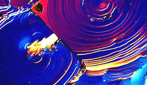
Figure 1. GdBa2Cu3O7 Differential Interference Contrast (DIC) reflected light photomicrograph of the surface of a single crystal of GdBa2Cu3O7. |
THE MEISSNER EFFECT
One of the most important manifestations of the new high temperature superconducting ceramics is their ability to exclude magnetic fields while in the superconducting state. This property was first recognized in 1933 by a German physicist, Meissner, and, rather than the drop to zero resistance, is the key element used in the demonstration of the superconducting effect. The Meissner effect is the reason behind the levitating of a magnet by a superconductor. The superconductor behaves essentially as a "magnetic mirror", perfectly reflecting the magnetic field lines back to the magnet. The repulsion causes the magnet to rise above the superconductor with it's height being determined by the balance between the field strength and weight of the magnet. This effect is responsible for a host of new applications in electromechanical devices such a frictionless bearings, levitated trains, and superefficient motors.
CURRENT RESEARCH
The most thoroughly studied superconductor is YBa2Cu3O7-x, more commonly known as 123 (2, 4). Although this ceramic is not the record holder (it superconducts at 90K), it is perhaps the best understood high temperature superconductor. Much of the current research on ceramic superconductors is now being focused on increasing the current handling capabilities of these materials. In it's most common form of a pellet pressed into shape from ground powder, the 123 ceramic is only capable of carrying currents a little stronger than 100 amperes per square centimeter and even this weak current will vanish in the presence of a magnetic field of just 0.1 tesla(4). Researchers found, that by partially melting and recooling the pellets, the grain boundaries were restructured and they have pushed the current density to 105 amperes per square centimeter. This is good enough for magnet applications. Still higher current densities have been obtained on epitaxially grown thin films through techniques such as Molecular Beam Epitaxy (MBE), laser ablation, and Metal-Organic Chemical Vapor Deposition (MOCVD).
MICROSCOPY OF SUPERCONDUCTING CERAMICS
At the National High Magnetic Field Laboratory (NHMFL) and the Center for Materials Research and Technology (MARTECH) at the Florida State University, we have been concentrating on optical, electron, and scanning probe microscopy of high temperature superconducting ceramics. These materials readily lend themselves to optical and electron microscopy, and several important advances have been made recently in scanning probe microscopy of the 123 superconducting ceramic.
The ceramic superconductors are all very dark materials with a high degree of reflectivity. Using reflected differential interference contrast microscopy, many details can be elucidated from examination of the surface structure in platelets of the superconductors. Although it has been reported that reflected polarized light microscopy can be utilized to characterize the nature of a superconductor simply by color, we have not found this to be reliable. Color differences usually can be attributed to thickness variations in the thin sheets which compose the platelets of the superconductors.
|
DIC reflected light photomicrograph of the surface features displayed by the non-superconducting PrBa2Cu3O7-x. |
Figure 1 illustrates the ab plane surface on a single crystal of the Gadolinium derivative of 123 where Gd is substituted for Yttrium. The primary surface features are a set of twin spiral dislocation growth patterns that are typically present on the surface of ceramic superconductors bearing the empirical formula: XBa2Cu3O7-x, where X can be Yttrium (Y), Gadolinium (Gd), and practically every other Rare Earth element with the surprising exception of Praseodymium (Pr). Single crystals of PrBa2Cu3O7-X contain many features in common with the rest of this class of ceramics including spiral dislocation growth patterns and twinning patterns with kink boundaries similar to those illustrated in Figure 2. The fact that this derivative does not superconduct, but instead acts as an electrical insulator, has led a number of researchers to investigate this material to obtain clues to the nature of superconductivity in this class of ceramics.
The original polarized transmitted light micrographs of powdered crystallites of the 123 superconductor revealed the presence of an extraneous substance composed of green rather than black crystals. After careful separation of the two substances, it was found that the green crystallites did not display any superconductivity and were an unwanted byproduct. Subsequently, by modifying the cooling process during the production of the superconductor, the unwanted green crystallites were eliminated.
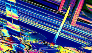
|
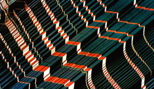
Transmitted polarised light micrograph illustrating twinning in a 0.5mm-thick wafer of Lanthanum Aluminate (LaAlO3).x19. |
Currently, we are attempting to prepare petrographic-type thin sections of the ceramic materials which have been fired in crucibles. These thin sections may allow us to determine grain structure characteristics and melt inclusions and allow the detection of cracks and fractures in transmitted polarized and differential interference contrast microscopy. The samples are prepared in a manner similar to that for geological petrographic thin sections. A diamond saw blade is first used to cut the tough ceramic from the bottom of the crucible. Next, the sample is impregnated with epoxy and mounted onto a microscope slide and then ground flat with silicon carbide followed by polishing with diamond. Finally, the specimen is ground to an approximate thickness of 100 µm microns and followed by hand polishing to a 30 µm thickness using diamond paste on bond paper.
Additional optical microscopy applications in ceramic superconductor research are the examination of thin films deposited onto epitaxial surfaces by MBE and MOCVD. The photomicrograph illustrated in Figure 3 is a transmitted light micrograph of a thin wafer of the material lanthanum aluminate (LaAlO3). This ceramic is a member of the perovskite family and although it does not superconduct, it is a good lattice match for thin film deposition of the 123 superconductor by the epitaxial methods described above. The stair-step twinning, quite evident in this photomicrograph, interferes with confluent epitaxial thin film deposition and researchers are hurriedly trying to develop similar materials that are devoid of these defects.
During recent laser ablation experiments, researchers were finding anomalous effects demonstrated by thin films of the 123 superconductor grown on lanthanum aluminate crystals. Upon microscopic examination, a series of "holes" were discovered in the films. Subsequent events led to the conclusion that the lanthanum aluminate crystals were contaminated by fingerprints and the superconductor was interrupted from epitaxial deposition by oily deposits on the crystal surface.
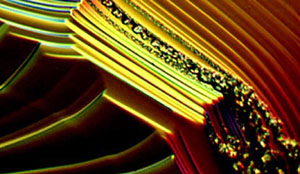
Another application of the ceramic superconductors is the preparation of thick films on alumina by a silk-screening process. In this procedure, the 123 ceramic is ground into a fine powder and transferred onto the alumina substrate. The resulting combination is then fired at 950°C for 10 hours followed by slow cooling in an oxygenated atmosphere. Thick films should be useful as devices to monitor minute magnetic properties in a variety of materials including biological specimens. Figure 4 illustrates a very high magnification photomicrograph of a 123 thick film on alumina. Note non-uniformity of the film as manifested by the larger particles fused into a formless matrix.
Transmission electron microscopy and Scanning Electron Microprobe elemental analysis have played a paramount role in the structural studies on the new high temperature superconducting ceramics. High resolution transmission electron microscopy has revealed the atomic structure of several superconductors in very thin section. These studies have confirmed X-ray diffraction experiments designed to elucidate the crystal structure in this highly unusual class of perovskites (4).
|
Reflected DIC photomicrograph of a thick film of YBa2Cu3O7-x. |
At MARTECH we routinely analyze the composition of newly synthesized ceramic superconductors using electron microprobe elemental analysis. This technique is complemented by the results obtained by X-ray diffraction powder pattern experiments and allows the close monitoring of the composition of these important ceramics.
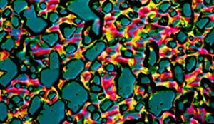
Another well-studied class of ceramic superconductors is a class of materials related to Bi2Sr2CaCu2Ox (usually abbreviated as 2212) (3), another copper oxide superconductor. These materials superconduct at 125-130K and represent the highest critical temperature superconductor family. In many ways the 2212 class of superconducting ceramics is very similar to the 123 class. The surfaces of 2212 ceramics are highly reflective and are easily examined using reflected light microscopy. Figure 5 illustrates the surface of a single crystal of 2212 showing striations in the multi-layered material. Spiral growth dislocation defects are not very common in this class of materials.
Scanning tunneling microscopy has revealed details of the surface structure of several ceramic superconductors at the atomic level. By cleaving the materials in different orientations, several crystalline patterns have emerged. This technique has also been employed to monitor the epitaxial thin film growth of superconductors by MBE and MOCVD. Recently two independent research teams confirmed an unusual phenomena in superconductor thin films using the tunneling microscopy technique. Chris Gerber and his coworkers at the IBM Zürich Research Laboratory in Switzerland reported (5) that thin films of the 123 superconductor contain several billion spiral dislocations (a com-mon crystalline growth pattern) per square inch. Almost simultaneously, Marilyn Hawley and her co-workers at the National High Magnetic Field's sister facility in the Los Alamos (New Mexico) National Laboratory reported nearly identical findings (6). These strikingly similar results indicate that the films start out as islands of material that do not build layer-by-layer as originally speculated. The islands actually grow by spiraling outward until the spirals merge with adjacent islands.
|
Reflected DIC photomicrograph of the ab plane surface of a single crystal of Bi2Sr2CaCu2Ox. |
THE FUTURE
The general restrictions on the possible limits of the critical temperature in superconducting ceramics are not known. Several families of superconductors with critical temperatures ranging from 30K to 125K have already been discovered, and this is not including the unstable and nonreproducible materials with apparently even higher critical temperatures. From this, we can conclude that many very good reasons exist for a continued search for new kinds of superconducting materials.
Recently, doped buckminister-fullerenes, commonly termed "buckeyballs" have been demonstrated to superconduct at somewhat low temperatures. These unusual hydrocarbons are composed of 60 carbon atoms arranged in a soccer-ball type structure first described by Buckminister Fuller. Scanning tunneling microscopy has demonstrated that buckeyballs can arrange themselves in a crystalline lattice and with the proper doping agent, may well prove to be an important class of superconductors.
Regardless of whatever turn the quest for new high temperature superconductors takes, it is for certain that this important field will remain very active for some time to come.
ACKNOWLEDGEMENTS
I would like to thank the National High Magnetic Field Laboratory (NHMFL), the superconductor Computations Research Institute (SCRI), and the Center for Materials Research and Technology (MARTECH) for supporting this work. Microscopes were kindly provided by Lynda Ruf and Stephen Page of the Nikon Instrument Group in Melville, New York.
Author's details
Michael W. Davidson, Research Scientist, Institute of Molecular Biophysics (IBM), The Florida State University, Tallahassee, Florida 32306, USA. Telephone: 850-6414-0542.
REFERENCES
1. Bednorz, J. and Mueller, K., "Possible High Tc Superconductivity in the Ba-La-Cu-O System", Zeitscrift fur Physik B, 64, 189 (1986).
2. Wu, M., Ashburn, J., Torng, C., Hor, P., Meng, L., Gao, L., Huang, Z., Wang, Y., and Chu, C., "Superconductivity at 93K in a New Mixed-Phase Y-Ba-Cu-O Compound System at Ambient Pressure, Physical Review Letters, 58, 908 (1987).
3. Engler, E., "Superconductivity at Accessible Temperatures", Chemtech, September page 542 (1987).
4. Hazen, R., "Perovskites", Scientific American 258, 74 (1988).
5. Gerber, C., Anselmetti, D., Bednorz, J., Mannhart, J., and Schlom, D., "Growth Sprials in YBa2Cu3O7-x Thin Films", Nature, 350, 279 (1991).
6. Hawley, M., Raistrick, K., Beery, J. and Houlton, R., "STM of Thin Film Superconductors", Science, 251, 1587 (1991).