 |
||
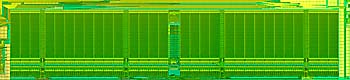
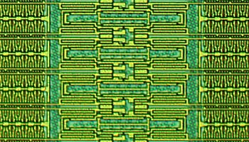
Layout of the Icach shown at x 37 magnifying factor. Only diffusion areas are visible. Green areas are N-diffusions and yellow are P-diffusions.
Metal 1 lines shown at x 10 magnification.

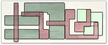
Diffusion areas shown at the x 10 magnification.
Metal 1 lines shown at x 20 magnification.
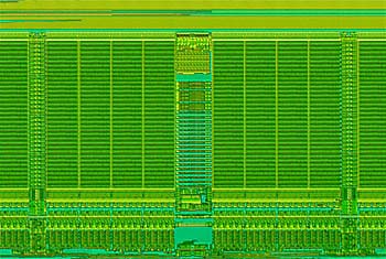
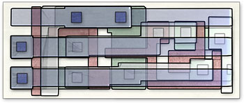
Diffusion areas shown at the x 20 magnification.
Metal 1 lines shown at x 50 magnification.
Diffusion areas shown at the x 50 magnification.
Metal1 layer
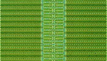
Diffusions layers
Metal 2 layer
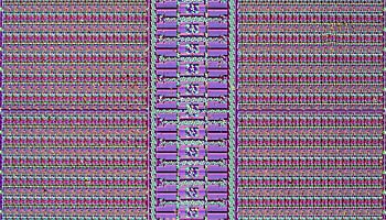
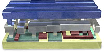
All layers shown at magnification factor of x 1,000
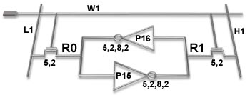
Schematics of the memory ICACH cell has total of 6 transistors and because of that it is called 6T cell. W1 line is word line. When this line is high it switches on transistors T1 and T2 and opposite binary values from lines L1 and H1 are written into the cell. Two back to back connected inverters statically hold the value which is written in.
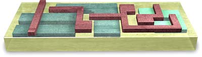
Layout of the 6T memory cell. Only polysilicon lines and diffusions are shown. The cell is shown with x 8,000 magnifing factor.
Layout of the same cell with the both metal lines shown.
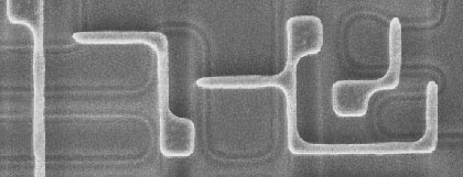
SEM picture shown at the same magnification factor. We can see that real shapes are far from being rectangular.
BACK TO ANATOMY OF THE MICROPROCESSOR HOME