Cyrix Integrated Circuits
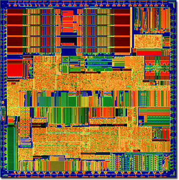
6x86 Microprocessor Die Polysilicon Layer
The digital image presented below reveals surface detail present on a complete Cyrix 6x86 microprocessor die at the polysilicon stage of fabrication. Bus lines, registers, and memory caches were highlighted using tungsten light filtered with red, green, blue, and yellow gels in oblique illumination.

Designed as a sixth-generation microprocessor to complete with Intel's Pentium line-up, the Cyrix 6x86 offered a number of advanced features compared to other processors of the time period. The chip contained a 3x bus-to-core clock multiplier that enabled instructions to be shuttled back and forth at accelerated rates, and a 16 kilobyte write-back level-one cache onboard the chip. Instruction sets were fully compatible with x86 operating systems and software, including Windows 95 and NT, and was also designed to work with competing OS/2, DOS, Solaris, and UNIX.
BACK TO CYRIX INTEGRATED CIRCUITS