
Polarized Light Digital Image Gallery
Diamond Thin Films
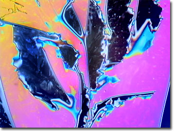
Chemical engineers create diamond thin films by sowing carbon atoms on a surface of silicon carbide. The miniature diamonds grow into interlocking molecular tetrahedrons, basically pyramids with triangles at their base.
View a second image of the diamond thin film.
Unlike their precious status as expensive ornamental jewels, thin films of diamonds and sapphires have industrial applications. Diamonds are known as an ultra-hard material for abrasive applications and for cutting. Unbreakable coatings and computer chips that can operate at very high temperatures are some of the promised applications of diamond thin films. In an idealized perfect diamond coating, the carbon atom tetrahedrons would be the same size and would line up with one another, forming a smooth layer. Crystals that grow at different rates create an imperfect thin layer with more limited abilities.
Diamond films are expected to be the most promising of the semiconducting materials. Using chemical vapor deposition, semiconductor manufacturers can create synthesized diamond films with desired textures and surface morphologies. To improve the electronic characteristics of a diamond thin film, the engineer wishes to employ highly oriented epitaxial diamond films, instead of randomly oriented polycrystalline films. Diamond films excel in active switching devices and high-power transistors, as well as in passive sensors including thermistors, pressure sensors, and radiation detectors. Applications demanding chemical electrodes (as in chemical and biological sensors) successfully employ diamond thin film semiconductors. The heat resistance of diamond films makes them well adapted for use in high-temperature chips found in automobile and aircraft engines, and household appliances such as microwave and conventional ovens and stoves and clothes dryers. In the power and communications fields, diamond thin films feature high breakdown fields and high carrier mobility, with large saturation velocities. The future is shining on synthesized diamond thin films and they will certainly be valuable to the economy and everyday lives of millions, even if they are not as in such short supply as their natural and brilliant gemstone siblings.
Contributing Authors
Omar Alvarado, Thomas J. Fellers and Michael W. Davidson - National High Magnetic Field Laboratory, 1800 East Paul Dirac Dr., The Florida State University, Tallahassee, Florida, 32310.
BACK TO THE POLARIZED LIGHT IMAGE GALLERY
BACK TO THE DIGITAL IMAGE GALLERIES
Questions or comments? Send us an email.
© 1995-2025 by Michael W. Davidson and The Florida State University. All Rights Reserved. No images, graphics, software, scripts, or applets may be reproduced or used in any manner without permission from the copyright holders. Use of this website means you agree to all of the Legal Terms and Conditions set forth by the owners.
This website is maintained by our
Graphics & Web Programming Team
in collaboration with Optical Microscopy at the
National High Magnetic Field Laboratory.
Last Modification Friday, Nov 13, 2015 at 02:19 PM
Access Count Since September 17, 2002: 10085
Visit the website of our partner in introductory microscopy education:
|
|