Integrated Circuit Image Gallery
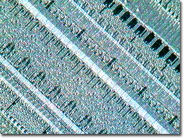
Intel 8088 Microprocessor
The 8088 was the processor that fueled the personal computer revolution beginning with the IBM PC introduced in 1981. Squeezing 29,000 transistors onto a sliver of silicon using 3.0 micron technology, the Intel 8088 central processing unit (CPU) was produced in two versions: one with a clock speed of 5 MHz capable of 0.33 MIPS (millions of instructions per second) and the other at 8 MHz and 0.75 MIPS. With a 16-bit internal register width, this microprocessor was able to address 1 megabyte of memory.

View a second image of the Intel 8088 Microprocessor.
View a third image of the Intel 8088 Microprocessor.
Intel's first venture in 16-bit computing, the 8086, was not related to the previous silicon electronic devices (4004, 8008, 8080). It featured a new instruction set and different hardware architecture. As a clear case of the semiconductor engineers getting ahead of other hardware and software designers, and because of difficulties connecting to peripherals, the 8086 processor was largely left abandoned. The 8088 was the answer, internally an 8086 with a more versatile 8-bit external bus and marketed at a lower price. The 8088 was Intel's first really successful CPU because it was adopted by IBM for their PC and XT models and by most XT-class clones. Originally produced with simple, but energy-hungry N-channel metal oxide semiconductor (NMOS) technology, the 8086 and 8088 chips were produced by Intel in the more up-to-date complementary metal oxide semiconductor (CMOS) fabrication techniques as the low-voltage 80c86 and 80c88, respectively for the newly arrived battery-powered notebook and sub-notebook computers.
During its fledgling years, Intel had to have other, more established semiconductor manufacturers produce its chips like the 8088 since computer manufacturers such as IBM did not want to bet their entire personal computer line on an unproven entity. Japanese semiconductor pioneer NEC also made the 8088. They later tired of simply licensing rights and designs from Intel and reverse-engineered the processor to create the NEC V20. The V20 was more efficient than the 8088 (increased clock speed), while maintaining complete compatibility and using the same command set as the 8088 processor.
Contributing Authors
Omar Alvarado, Thomas J. Fellers and Michael W. Davidson - National High Magnetic Field Laboratory, 1800 East Paul Dirac Dr., The Florida State University, Tallahassee, Florida, 32310.
BACK TO THE INTEGRATED CIRCUIT IMAGE GALLERY
BACK TO THE DIGITAL IMAGE GALLERIES
Questions or comments? Send us an email.
© 1995-2025 by Michael W. Davidson and The Florida State University. All Rights Reserved. No images, graphics, software, scripts, or applets may be reproduced or used in any manner without permission from the copyright holders. Use of this website means you agree to all of the Legal Terms and Conditions set forth by the owners.
This website is maintained by our
Graphics & Web Programming Team
in collaboration with Optical Microscopy at the
National High Magnetic Field Laboratory.
Last Modification Friday, Nov 13, 2015 at 02:19 PM
Access Count Since September 17, 2002: 9737
Visit the website of our partner in introductory microscopy education:
|
|
