
Integrated Circuit Image Gallery
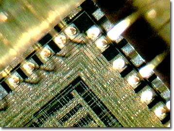
Intel 486SX Microprocessor
While the 80486 (DX version) is basically an enhanced 386 with an internal cache and math coprocessor, the Intel 486SX is the "economy model" lacking the math processor and internal cache. Originally issued as discounted DX chips that failed the cache and/or coprocessor tests, these defective silicon chips were soon released as their own design in a fashion similar to Intel's release of the 386SX following the higher-power 80386 processor (386DX).
View a second image of the Intel 486SX.
Intel squeezed 1.185 million transistors onto a 67-square-millimeter die applying 1.0-micron complementary metal oxide semiconductor (CMOS) fabrication techniques. The Intel 486SX central processing unit (CPU) was released in September 1991 in three models with different clock speeds: 16 MHz, 20 MHz, and 25 MHz versions. All had 32-bit internal registers and external bus widths, could address up to four gigabytes of memory, and maintained backward compatibility with previous CPUs and operating systems. By the following year, Intel released a 33 MHz-clock-speed version with a reduced number of transistors (900,000) using the more advanced 0.8-micron photolithography processes. The newer 486SX-33 MHz was capable of performing 27 million instructions per second (MIPS).
The 486SX microprocessor is referred to by some users as "cripple ware": hardware that is deliberately disabled by the manufacturer and which can supposedly be upgraded to the more expensive model (the 486DX in this case) by some trivial change such as removing a jumper. In fact, many SX owners were the victims of a terrible April Fool's Day prank by a German computer magazine, which reported that by carefully drilling a hole of a specified diameter through the right point on the chip, the disabling circuit would break, reactivating the floating-point unit (FPU). Some people actually attempted this extreme "adjustment" and were then forced to replace their processors. In the case of the initially defective 80486s, Intel used a laser to destroy the FPU connections before shipping them.
Contributing Authors
Omar Alvarado, Thomas J. Fellers and Michael W. Davidson - National High Magnetic Field Laboratory, 1800 East Paul Dirac Dr., The Florida State University, Tallahassee, Florida, 32310.
BACK TO THE INTEGRATED CIRCUIT IMAGE GALLERY
BACK TO THE DIGITAL IMAGE GALLERIES
Questions or comments? Send us an email.
© 1995-2025 by Michael W. Davidson and The Florida State University. All Rights Reserved. No images, graphics, software, scripts, or applets may be reproduced or used in any manner without permission from the copyright holders. Use of this website means you agree to all of the Legal Terms and Conditions set forth by the owners.
This website is maintained by our
Graphics & Web Programming Team
in collaboration with Optical Microscopy at the
National High Magnetic Field Laboratory.
Last Modification Friday, Nov 13, 2015 at 02:19 PM
Access Count Since September 17, 2002: 8145
Visit the website of our partner in introductory microscopy education:
|
|