Integrated Circuit Image Gallery
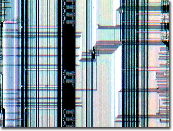
IBM 386SLC Microprocessor
As a low-power version of the stellar 386 microprocessor released in late 1991, the IBM 386SLC was equipped with extra pins assigned for power management and a software-enabled 8-Kbyte cache memory. Designed with complementary metal oxide semiconductor (CMOS) technology, the 161-square millimeter die featured three models with clock speeds of 16, 20, and 25 MHz. The fastest model produced only 2.5 watts of dissipated power, suiting it well for laptops and other portable devices.

View a low magnification image of the IBM 386SLC processor.
View a medium magnification image of the IBM 386SLC processor.
Released in 1992, the IBM PS/2 (Models 35 and 40 SLC) was often outfitted with the IBM 386SLC processor as that company's first attempt to improve the performance of 386SX-based systems without having to replace the system boards. Coupled with a Cyrix 83S87 math coprocessor, the addition of an internal cache of 16 kilobytes of memory, and optional random access memory up to 16 Mbytes, the processor provided roughly a 50-percent improvement in performance over a typical 386SX/20-based system. Still, the 386SLC-based computers were limited because of slow and narrow memory interfaces.
The SLC versions of the 386 chip featured additional power management modes that conserved batteries for extended use in portable computing applications and garnered "Green Machine" awards. The IBM 386SLC differed from Intel's i386SL and its clones by virtue of the on-chip 16-kilobyte cache memory. IBM also marketed upgrade units for their highly successful IBM PS/2 Model 25, as the IBM 7386 planar model, which was equipped with an 80386SLC processor operating at 20 MHz clock speed. Tapping into the older 8086, 286, or 386SX-based system's hard drive and utilizing existing peripherals, this unusual upgrade solution provided SVGA video and a maximum of 16 Mbytes of system memory packaged in four 4-Mbyte parity single-in-line memory modules (SIMMs).
Contributing Authors
Omar Alvarado, Thomas J. Fellers and Michael W. Davidson - National High Magnetic Field Laboratory, 1800 East Paul Dirac Dr., The Florida State University, Tallahassee, Florida, 32310.
BACK TO THE INTEGRATED CIRCUIT IMAGE GALLERY
BACK TO THE DIGITAL IMAGE GALLERIES
Questions or comments? Send us an email.
© 1995-2025 by Michael W. Davidson and The Florida State University. All Rights Reserved. No images, graphics, software, scripts, or applets may be reproduced or used in any manner without permission from the copyright holders. Use of this website means you agree to all of the Legal Terms and Conditions set forth by the owners.
This website is maintained by our
Graphics & Web Programming Team
in collaboration with Optical Microscopy at the
National High Magnetic Field Laboratory.
Last Modification Friday, Nov 13, 2015 at 02:19 PM
Access Count Since September 17, 2002: 8771
Visit the website of our partner in introductory microscopy education:
|
|
