
Integrated Circuit Image Gallery
Dual-Ported RAM Controller
During the beginning of the 80X86 era of the early 1980s, dual-port random access memory (RAM) controller chips, such as the Intel 8207, were marketed in large quantities. As the name implies, these semiconductor devices arbitrate RAM requests from the central processing unit (CPU) and other devices such as a math coprocessor in a personal computer, electronic game console, hand-held device, or other processor-controlled hardware.
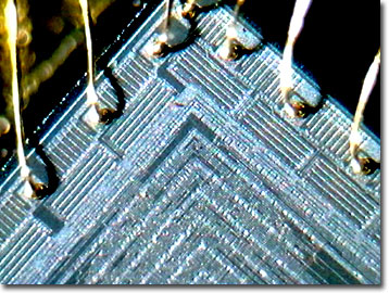
Also known as shared-storage interface chips, dual-ported RAM controllers provide more efficient use of on-board read/write storage by multiple devices without the increased costs, complexity, and size of redundant memory chips. These controllers still play a function in some consumer electronic devices and industrial processes that depend on embedded processors such as the 80C186. By controlling the cycle time at the nanosecond level, the data rate for the random access memory is optimized at a speed that neither of the sharing processors can achieve. If a request for memory is made and the RAM is already in use and is of higher priority, the new RAM request is placed in a wait state until the memory is freed.
More advanced microprocessors that combine floating-point units (FPUs) with the CPU on a single chip eliminated much of the demand for dual-ported RAM controllers in personal computers. IBM's approach used complementary metal oxide semiconductor (CMOS) fabrication techniques to create an array of 10,000 gates for their shared-storage interface chip. The IBM chip adapts to both 8-bit and 16-bit data bases that may be found on a system unit bus. All data communications between the system unit and the coprocessor adaptor are completed through these interfaces. IBM's dual-ported RAM controller additionally provides checking for parity and timer errors. It is designed for up to 1,024 kilobytes of RAM storage (128 8-kilobyte pages) and uses a 25-MHz clock for sampling RAM requests.
Contributing Authors
Omar Alvarado, Thomas J. Fellers and Michael W. Davidson - National High Magnetic Field Laboratory, 1800 East Paul Dirac Dr., The Florida State University, Tallahassee, Florida, 32310.
BACK TO THE INTEGRATED CIRCUIT IMAGE GALLERY
BACK TO THE DIGITAL IMAGE GALLERIES
Questions or comments? Send us an email.
© 1995-2025 by Michael W. Davidson and The Florida State University. All Rights Reserved. No images, graphics, software, scripts, or applets may be reproduced or used in any manner without permission from the copyright holders. Use of this website means you agree to all of the Legal Terms and Conditions set forth by the owners.
This website is maintained by our
Graphics & Web Programming Team
in collaboration with Optical Microscopy at the
National High Magnetic Field Laboratory.
Last Modification Friday, Nov 13, 2015 at 02:19 PM
Access Count Since September 17, 2002: 12247
Visit the website of our partner in introductory microscopy education:
|
|