
Interactive Tutorials
Solar Cell Operation
Solar cells convert light energy into electrical energy either indirectly by first converting it into heat, or through a direct process known as the photovoltaic effect. The most common types of solar cells are based on the photovoltaic effect, which occurs when light falling on a two-layer semiconductor material produces a potential difference, or voltage, between the two layers. The voltage produced in the cell is capable of driving a current through an external electrical circuit that can be utilized to power electrical devices. This tutorial explores the basic concepts behind solar cell operation.
The tutorial initializes at an arbitrarily set "medium" photon intensity level, with photons randomly impacting the surface of the solar cell to generate free electrons. The released electrons complete a simple circuit containing two light bulbs that become illuminated when current flows through. In order to increase or decrease the photon flux, use the Photon Intensity slider to adjust the number of photons incident on the surface.
Today, the most common photovoltaic cells employ several layers of doped silicon, the same semiconductor material used to make computer chips. Their function depends upon the movement of charge-carrying entities between successive silicon layers. In pure silicon, when sufficient energy is added (for example, by heating), some electrons in the silicon atoms can break free from their bonds in the crystal, leaving behind a hole in an atom's electronic structure. These freed electrons move about randomly through the solid material searching for another hole with which to combine and release their excess energy. Functioning as free carriers, the electrons are capable of producing an electrical current, although in pure silicon there are so few of them that current levels would be insignificant. However, silicon can be modified by adding specific impurities that will either increase the number of free electrons (n-silicon), or the number of holes (missing electrons; also referred to as p-silicon). Because both holes and electrons are mobile within the fixed silicon crystalline lattice, they can combine to neutralize each other under the influence of an electrical potential. Silicon that has been doped in this manner has sufficient photosensitivity to be useful in photovoltaic applications.
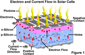
In a typical photovoltaic cell, two layers of doped silicon semiconductor are tightly bonded together (illustrated in Figure 1). One layer is modified to have excess free electrons (termed an n-layer), while the other layer is treated to have an excess of electron holes or vacancies (a p-layer). When the two dissimilar semiconductor layers are joined at a common boundary, the free electrons in the n-layer cross into the p-layer in an attempt to fill the electron holes. The combining of electrons and holes at the p-n junction creates a barrier that makes it increasingly difficult for additional electrons to cross. As the electrical imbalance reaches an equilibrium condition, a fixed electric field results across the boundary separating the two sides.
When light of an appropriate wavelength (and energy) strikes the layered cell and is absorbed, electrons are freed to travel randomly. Electrons close to the boundary (the p-n junction) can be swept across the junction by the fixed field. Because the electrons can easily cross the boundary, but cannot return in the other direction (against the field gradient), a charge imbalance results between the two semiconductor regions. Electrons being swept into the n-layer by the localized effects of the fixed field have a natural tendency to leave the layer in order to correct the charge imbalance. Towards this end, the electrons will follow another path if one is available. By providing an external circuit by which the electrons can return to the other layer, a current flow is produced that will continue as long as light strikes the solar cell. In the construction of a photovoltaic cell, metal contact layers are applied to the outer faces of the two semiconductor layers, and provide a path to the external circuit that connects the two layers. The final result is production of electrical power derived directly from the energy of light.
The voltage produced by solar cells varies with the wavelength of incident light, but typical cells are designed to use the broad spectrum of daylight provided by the sun. The amount of energy produced by the cell is wavelength-dependent with longer wavelengths generating less electricity than shorter wavelengths. Because commonly available cells produce only about as much voltage as a flashlight battery, hundreds or even thousands must be coupled together in order to produce enough electricity for demanding applications. A number of solar-powered automobiles have been built and successfully operated at highway speeds through the use of a large number of solar cells. In 1981, an aircraft known as the Solar Challenger, which was covered with 16,000 solar cells producing over 3,000 watts of power, was flown across the English Channel powered solely by sunlight. Feats such as these inspire interest in expanding the uses of solar power. However, the use of solar cells is still in its infancy, and these energy sources are still largely restricted to powering low demand devices.
Current photovoltaic cells employing the latest advances in doped silicon semiconductors convert a average of 18 percent (reaching a maximum of about 25 percent) of the incident light energy into electricity, compared to about 6 percent for cells produced in the 1950s. In addition to improvements in efficiency, new methods are also being devised to produce cells that are less expensive than those made from single crystal silicon. Such improvements include silicon films that are grown on much less expensive polycrystalline silicon wafers. Amorphous silicon has also been tried with some success, as has the evaporation of thin silicon films onto glass substrates. Materials other than silicon, such as gallium arsenide, cadmium telluride, and copper indium diselenide, are being investigated for their potential benefits in solar cell applications. Recently, titanium dioxide thin films have been developed for potential photovoltaic cell construction. These transparent films are particularly interesting because they can also serve double duty as windows.
Contributing Authors
Matthew J. Parry-Hill, Robert T. Sutter and Michael W. Davidson - National High Magnetic Field Laboratory, 1800 East Paul Dirac Dr., The Florida State University, Tallahassee, Florida, 32310.