
Interactive Tutorials
Light Emitting Diodes
Light emitting diodes (LEDs) are a general source of continuous light with a high luminescence efficiency, and are based on the general properties of a simple twin-element semiconductor diode encased in a clear epoxy dome that acts as a lens. This interactive tutorial explores how two dissimilar doped semiconductors can produce light when a voltage is applied to the junction region between the materials.
The tutorial initializes with a simple doped semiconductor p-n junction connected to a direct current (DC) voltage source (a D-cell battery) appearing in the window. The default p-type semiconductor material is doped gallium aluminum arsenide (GaAlAs), while the n-type semiconductor (layered onto the substrate) is composed of doped gallium arsenide (GaAs). Between the two doped semiconductors is an Active Layer that exists in an equilibrium state (without light being emitted) when no voltage is applied to the diode junction.
At initialization, the voltage applied to the junction is 2 volts (an arbitrary setting), and holes from the p-doped semiconductor region (GaAlAs) meet electrons from the n-doped region (GaAs) in the Active Layer to produce infrared light. In order to operate the tutorial, use the mouse cursor to translate the Voltage slider between a range of zero and four volts. As the voltage is increased, the number of holes and electrons entering the junction region increases, as does the amount of light (number of colored photons) being emitted when the holes and electrons combine. The composition of the materials comprising the doped semiconductor diode can be altered with the LED Material slider. As the slider is translated, the n-doped and p-doped materials change to new semiconductors that yield a variety of visible light wavelengths when electrons and holes meet and combine in the Active Layer region. The common name for each color of light produced by the diode is presented above the LED Material slider bar.
At the heart of a light emitting diode is a semiconductor chip fabricated in a manner similar to that of common integrated circuits, which are utilized a wide array of devices ranging from computers to household appliances. The diode semiconductor contains several very thin layers of material that are sequentially deposited onto a supporting substrate (usually silicon or doped gallium). In the tutorial, the first semiconductor material that is deposited onto the substrate is doped with atoms containing excess electrons to yield what is termed an n-type semiconductor. A second doped material, containing atoms having too few electrons (a p-type semiconductor), is then deposited onto the first semiconductor to form the diode. The region created between the doped semiconductor materials is known as the active layer.
When a voltage is applied to the diode, holes (positive charges) from the p-type region and electrons (negative charges) from the n-type region meet in the active layer to produce light. The wavelength of light emitted by the diode is dependent upon the chemical composition and relative energy levels of the doped semiconductor materials that comprise the p and n regions. By varying the composition of the doped semiconductors, a wide range of emitted wavelengths can be generated that represent every primary color in the visible light spectrum.
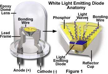
After being fabricated, the semiconductor diode chip is mounted in a reflector cup connected to a lead frame, and is bonded to the anode and cathode terminals of the frame through miniature bonding wires (see Figure 1). The entire assembly is then encased in a solid epoxy dome lens that enables emitted light to be focused in a single direction. Diffusion of light through the epoxy lens is controlled by embedding tiny glass particles into the lens that scatter light and spread the light beam emerging from the lens. Epoxy lenses can also be tinted with dyes to indicate the color of the diode when in the active (on) state. Clear epoxy lenses do not contain dyes or diffusing glass and produce the greatest amount of light output, but are limited to a very narrow viewing angle. The angle of the light cone emitted by the diode-reflector cup combination can be altered by changing the epoxy lens shape, the geometry of the reflector cup, and the size and distance between the semiconductor diode and the nose of the epoxy lens.
By varying the composition of the doped semiconductor materials utilized to fabricate the diode, common light emitting diodes can manufactured that emit light in both the visible and infrared wavelength regions. The most common semiconductors employed in diode construction are aluminum, arsenic, gallium, indium, phosphorous and nitrogen (as nitrides), which can be combined in a variety of different proportions and doping levels. The wavelength (color) of light produced by a light emitting diode is determined exclusively by the nature of the doped semiconductor materials and is independent of dyes utilized to color the epoxy dome lens. Typical visible wavelengths emitted by semiconductor diodes are red (650 nanometers), orange (620 nanometers), yellow (585 nanometers), green (555 nanometers), and blue (480 nanometers). White light LEDs are manufactured by a variety of mechanisms, but often contain a phosphor material in the reflector cup that intercepts high-energy blue light from the diode and emits secondary radiation across the entire visible light spectrum.
Contributing Authors
Robert T. Sutter and Michael W. Davidson - National High Magnetic Field Laboratory, 1800 East Paul Dirac Dr., The Florida State University, Tallahassee, Florida, 32310.
BACK TO SOURCES OF VISIBLE LIGHT