
Concepts in Digital Imaging Technology
Interline Transfer CCD Architecture
Interline charge-coupled device architecture is designed to compensate for many of the shortcomings of frame-transfer CCDs. These devices are composed of a hybrid structure incorporating a separate photodiode and an associated parallel readout CCD storage region into each pixel element. The functions of these two regions are isolated by a metallic mask structure placed over the light shielded parallel readout CCD elements.
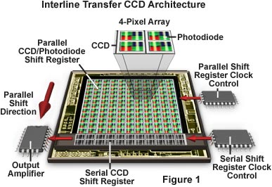
Masked regions of the pixels are positioned alongside the photodiode elements in an alternating parallel array traversing the length of the CCD's vertical axis. Photodiodes in the array comprise the image plane and collect incoming photons projected onto the CCD surface by the camera or microscope lenses. After image data has been collected and converted into electrical potential by the image array, the data is then quickly shifted in a parallel transfer to the adjacent CCD storage area of each pixel element. The storage portion of the pixel element is illustrated as a cluster of gray-scale elements covered with an opaque mask adjacent to the red, green, and blue photodiode elements in each CCD. These pixel elements combine to form vertical columns that run from the serial shift register to the top of the array grid. An enlarged view of a four-pixel array containing both photodiode and CCD elements appears in the upper portion of Figure 1.
| Interactive Java Tutorial | |||||||||||
|
|||||||||||
Like the full-frame and frame-transfer architectures, interline transfer CCDs undergo readout by shifting rows of image information in a parallel fashion, one row at a time, to the serial shift register. The serial register then sequentially shifts each row of image information to an output amplifier as a serial data stream. The entire process is repeated until all rows of image data are transferred to the output amplifier and off the chip to a analog-to-digital signal converter integrated circuit. Reconstruction of the image in a digital format yields the final photograph or photomicrograph.
During the period in which the parallel storage array is being read, the image array is busy integrating charge for the next image frame, similar to the operation of the frame-transfer CCD. A major advantage of this architecture is the ability of the interline transfer device to operate without a shutter or synchronized strobe, allowing for an increase in device speed and faster frame rates. Image "smear", a common problem with frame-transfer CCDs, is also reduced with interline CCD architecture because of the rapid speed (only one or a few microseconds) in which image transfer occurs. Drawbacks include a higher unit cost to produce chips with the more complex architecture, and a lower sensitivity due to a decrease in photosensitive area present at each pixel site. This shortcoming can be partially overcome by incorporation of microlenses (or lenslets) on the photodiode array complex to increase the amount of light entering each element. Interline devices with microlens enhancement typically increase the optical fill factor from approximately 20-25 percent to over 75 percent, dramatically improving the net quantum efficiency of the device in the visible light wavelength region.
Interline transfer CCDs experience sampling errors that are increased due to the reduced aperture size. In addition, a portion of the incident light can leak into CCD vertical registers, especially in brightfield applications where microscope lamp intensity is undiminished by the specimen. Some interline CCD designs experience image "lag" as a result of charge transfer time constant delays associated with transfer of charge from photodiodes to the CCD storage areas. This transfer delay results in a residual charge being left in the photodiodes that is added to the next frame, resulting in an "after-image" artifact. Newer hole-accumulation charge-coupled devices are capable of complete transfer, thus eliminating image lag.
Contributing Authors
Mortimer Abramowitz - Olympus America, Inc., Two Corporate Center Drive., Melville, New York, 11747.
Michael W. Davidson - National High Magnetic Field Laboratory, 1800 East Paul Dirac Dr., The Florida State University, Tallahassee, Florida, 32310.
BACK TO CONCEPTS IN DIGITAL IMAGING TECHNOLOGY