Integrated Circuit Image Gallery
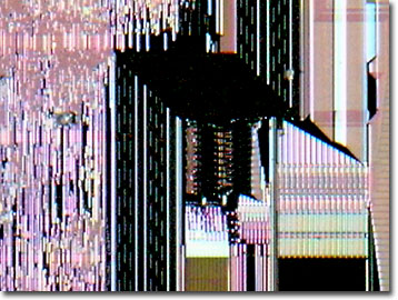
Advanced Micro Devices 486DX4 Microprocessor
The involvement of semiconductor manufacturer Advanced Micro Devices (AMD) in personal computing spans the entire history of the industry, having supplied every generation of PC processor from the 8088 used in the first IBM PCs to the newer, seventh generation 1.4 GHz clock speed Athlon processor. It wasn't until AMD and its rival Cyrix released their clone versions of the Intel 486DX2 and 486DX4 microprocessors that they really came into their own.

The AMD 486DX4 100 MHz is a 32-bit central processing unit (CPU) that features clock tripling where the internal processor clock speed is three times the speed of the memory bus and the motherboard, which have a bus speed of 33 MHz. Note that, despite the name, the DX4 does not run at four times the memory bus speed. The "DX3" was an Intel designation for a 2.5X clock multiplier for the 486 microprocessor family that was never marketed.
Although referred to as a "clone", the Advanced Micro Devices chip featured a cooler-operating 3.3-volt internal power requirement and power management features that favored its use in portable computers. This advanced chip also garnered a "green" rating by the U.S. Environmental Protection Agency in their Energy Star program with a 40 percent power reduction, compared to the Intel version, which produced a much-greater 7.0 watts, and required fans and heat sinks for cooling. The 80486DX4 120 MHz was an AMD processor that tripled their 40-MHz external clock speed, and was a model not available from Intel. To achieve new clock speeds, Intel engineers increased the number of transistors to 1.6 million and reduced the original 1.0-micron fabrication technology of the 486 down to a much narrower 0.6 microns. AMD answered with its own improved 3-layer, 0.5-micron complementary metal oxide semiconductor (CMOS) techniques that resulted in processors that only dissipated 2.6 watts of heat at 100 MHz, or 3.2 watts at 120 MHz clock speed.
Contributing Authors
Omar Alvarado, Thomas J. Fellers and Michael W. Davidson - National High Magnetic Field Laboratory, 1800 East Paul Dirac Dr., The Florida State University, Tallahassee, Florida, 32310.
BACK TO THE INTEGRATED CIRCUIT IMAGE GALLERY
BACK TO THE DIGITAL IMAGE GALLERIES
Questions or comments? Send us an email.
© 1995-2025 by Michael W. Davidson and The Florida State University. All Rights Reserved. No images, graphics, software, scripts, or applets may be reproduced or used in any manner without permission from the copyright holders. Use of this website means you agree to all of the Legal Terms and Conditions set forth by the owners.
This website is maintained by our
Graphics & Web Programming Team
in collaboration with Optical Microscopy at the
National High Magnetic Field Laboratory.
Last Modification Friday, Nov 13, 2015 at 02:19 PM
Access Count Since September 17, 2002: 13108
Visit the website of our partner in introductory microscopy education:
|
|
