
QX3 Digital Imaging System
At the heart of the Intel Play QX3 microscope is a digital imaging system centered around an active pixel sensor (APS) complementary metal oxide semiconductor (CMOS) integrated circuit designed and manufactured in Europe by VLSI Vision, Ltd., in Edinburgh, Scotland.
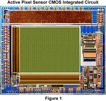
VLSI Vision was purchased early in 1999 by Europe's STMicroelectronics, one of the world's largest designers and manufacturers of CMOS semiconductor devices. The new company will continue to produce CMOS imaging products, which is becoming a fiercely competitive business with big name players such as Intel, Lucent, and Hewlett-Packard. The CMOS imaging chip used in the Intel QX3 microscope, a VLSI Vision VV6404 CIF ColorMOS sensor, is illustrated in Figure 1. In the center of the chip is a large array of optical sensors that are individual photodiode elements covered with dyed filters and arranged in a periodic matrix. A high magnification view of a single "pixel" element is shown in Figure 2(a). This group of four photodiodes contains filters based on the primary colors red, green, and blue.
Each photodiode is masked by either a red, green, or blue filter in low-end chips, but higher resolution CMOS devices often use a teal (blue-green) filter in place of one of the green filters. Together, the four elements illustrated in Figure 2(a) comprise the light-sensitive portion of the pixel. Two green filter masks are used because visible light has an average wavelength of 550 nanometers, which lies in the green color region. Each pixel element is controlled by a set of three transistors and an amplifier that work together to collect and organize distribution of optical information. The array is interconnected much like memory addresses and data busses on a DRAM chip so that the charge generated by photons striking each individual pixel can be accessed randomly to provide selective sampling of the CMOS sensor.
The individual amplifiers associated with each pixel help reduce noise and distortion levels, but they also induce an artifact known as "fixed pattern noise" that arises from small differences in the behavior of individual pixel amplifiers. This is manifested by reproducible patterns of "speckle" behavior in the image generated by CMOS active pixel sensor devices. A great deal of research effort has been invested in solving this problem, and the residual level of noise has been dramatically reduced in CMOS sensors such as the VV6404 ColorMOS. Another feature of CMOS active pixel sensors is the lack of column streaking due to pixel bloom when shift registers overflow. This problem is serious with the charged coupled devices (CCDs) found in most video camcorders. Another phenomenon, known as "smear", which is caused by charge transfer in CCD chips under illumination, is also absent in CMOS active pixel sensor devices.
A larger view of the photodiode elements present in the VV6404 is shown in Figure 2(b) where several pixel clusters are illustrated. Removal of the photodiodes and surface filters yields the underlying transistor, bus, and amplifier elements shown in Figure 2(c). The array in the VV6404 is 352 x 288 pixels in size and features an 11:12 aspect ratio, making it compliant with the Common Image Format (CIF) resolution size, which is a feature often found in chips of this type.
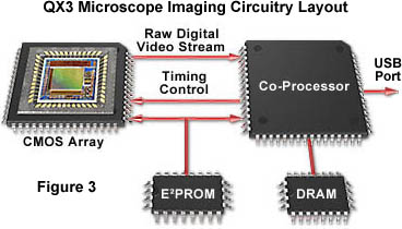
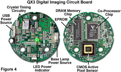
Assisting the CMOS VV6404 digital photodiode integrated circuit is a coprocessor that is matched to the APS CMOS to optimize the handling of image data. Together, the VV6404 and the coprocessor (termed the CPIA 1.5 by Vision), along with support circuitry, form a chipset that is the basis for a CIF-resolution digital camera with a Universal Serial Bus (USB) interface. This ingeniously crafted "camera-on-a-chip" fits onto a single circuit board (illustrated in Figure 4) that is housed within the QX3 microscope body. The CMOS sensor and coprocessor perform the key functions of image capture, digital video image processing, video compression, and interfacing to the USB computer bus system.
A schematic diagram of elements contained in the VV6404 chipset is presented in Figure 3. Light reflected from or passing through the specimen is magnified by lenses in the objective before being focused onto the photodiode array of the VV6404, where image data is captured by the circuitry of the chip. The system is initialized and controlled through an EEPROM programmable read-only memory chip that also receives information from the computer through the USB port. Timing functions for the circuitry are performed on the VV6404 with the assistance of several crystal oscillators placed elsewhere on the circuit board. The CPIA 1.5 coprocessor retrieves the image data from the CMOS sensor and then processes the data before passing it along to the USB port. Incorporated into the coprocessor is a proprietary digital video processor engine that is capable of performing automatic exposure and gain control, white balance, color matrixing, gamma correction, and aperture control.
The CPIA 1.5 coprocessor also features hardware video compression that is capable of producing real time video frame rates of 30 frames per second in CIF (352 x 288 pixels) resolution. This is accomplished because the CPIA 1.5 supports isochronous data transfer mode, which is an implement of the USB specification. Isochronous (derived from the Greek words for equal and time) processes refer to data transmissions that require exact timing coordination to be successful, such as multiplexing audio with digital video information. This transfer mode is useful in multimedia streams that demand data be delivered at the same rate as the computer display paint to ensure that audio is synchronized with the video. Both the high-performance universal serial bus and the asynchronous transfer mode (ATM) specifications support isochronous data transfer.
Response of the Intel QX3 is heavily dependent upon the color depth of the assisting computer monitor and the overall capabilities of the machine. Intel recommends a minimum system requirement of a 200 MHz Pentium processor or faster with 32 Mb RAM and a 800 x 600 pixel display with 16-bit color depth (65,536 colors). A computer bearly meeting these specifications will not perform well and will respond with delays in video while focusing the microscope or during time-lapse and real-time movie recording. We recommend a minimum of a 400 MHz Pentium II processor with 128 Mb RAM to avoid excessive video delays during routine operation of the microscope.
The video circuitry of the QX3 also contains a 4 Mb DRAM chip manufactured by Mosel Vitelic, which handles storage of images prior to transfer to the computer main RAM bank. This integrated circuit is designed specifically for low-power peripherial applications and is ideally suited for the QX3 computer microscope.
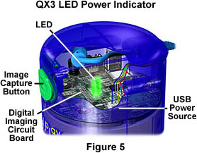
Another advantage of using CMOS optical sensors in peripherial devices such as the QX3 is their low power consumption requirements. Chips on the circuit board and the tungsten lamps of the QX3 require so little power that the microscope can take power directly from the USB input/output bus. In the central part of the circuit board is a green light emitting diode (LED) that indicates when the microscope is receiving power from the computer (as illustrated in Figure 5). If the microscope does not appear to be functioning, a quick glance at the LED will determine whether or not it is receiving power and hence, whether the USP cable is correctly inserted into the computer port.
As we have discussed, the CMOS active pixel sensor is an emerging technology that will push the limits on digital imaging both in toys and in the general consumer electronics market. Mass production of CMOS devices is very economical and many facilities that are currently engaged in fabrication of microprocessors, memory, and support chips can be easily converted to produce CMOS optical sensors. Although CCD chips were responsible for the rapid development of video camcorders, the technology has remained trapped as a specialized process that requires custom tooling outside the mainstream of integrated circuit fabrication. Also, the CCD devices require a substantial amount of support circuitry and it is not unusual to find five to six circuit boards in a typical video camcorder.
The primary concerns with CMOS technology are the rather low quality, noisy images that are obtained with respect to similar CCD devices. These are due primarily to process variations that produce a slightly different response in each pixel, which appears in the image as "snow". Another problem is the total amount of chip area that is sensitive to light is less in CMOS devices making them less sensitive to light. These problems will be overcome as process technology advances and it is very possible that CMOS devices will eclipse the CCD as the technology of choice in the very near future.
BACK TO INTEL PLAY QX3 MICROSCOPE ANATOMY
Questions or comments? Send us an email.
© 1995-2025 by Michael W. Davidson and The Florida State University. All Rights Reserved. No images, graphics, software, scripts, or applets may be reproduced or used in any manner without permission from the copyright holders. Use of this website means you agree to all of the Legal Terms and Conditions set forth by the owners.
This website is maintained by our
Graphics & Web Programming Team
in collaboration with Optical Microscopy at the
National High Magnetic Field Laboratory.
The QX3 microscope design is copyrighted © 2025 by Mattel, Inc. Intel® Play™ is a registered trademark of the Intel Corporation. These companies reserve all of their rights and privileges under copyright law. The material contained in this website is solely the opinion of the authors and is intended for eduational use only.
Last Modification Friday, Nov 13, 2015 at 02:18 PM
Access Count Since December 24, 1999: 56093
Visit the official Intel Play website:
![]()