The Magnetic Thin Film Collection

Nickel Oxide on Sodium Chloride
Magnetic Thin Films
|
Over the past few decades, there has been an intense level of research into the field of magnetic thin films, despite the fact that work with these intriguing materials began in the 1880s. One of the primary reasons for such heightened interest has been the advent of increasingly improved preparation techniques of the films. The two primary means of producing the films today are molecular beam epitaxy (MBE) and metal-organic chemical vapor deposition (MOCVD). The development of these methods began in 1968 when American scientist John Arthur reported that gallium arsenide could be grown by shooting a beam of gallium atoms and arsenic molecules toward the flat face of a crystal of the molecule. Though a variety of methods for creating thin films are currently in use today, typically the films are constructed atom-by-atom under very high vacuum conditions typically in the range of 10(E-11) Torr. Particle beams are prepared by thermal evaporation of Knudsen cells or electron-beam guns. The thickness of film formation is monitored with quartz crystals, optical detection methods, and mass spectrometers. 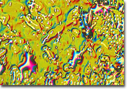
Iron Oxide on Indium Phosphide A particularly important issue in the fabrication of magnetic thin films is finding a magnetic material and substrate that are good lattice matches. If the lattices are well suited for one another and the application is carried out properly, the surface of a magnetic thin film resembles a mirror, its texture appearing smooth and flawless when examined using optical microscopy. If the spacing between atoms in the substrate is too different from that of the overlying film, however, then the film may exhibit wrinkling, clumping, or other deformities. Take for example the film illustrated in our banner, which was deposited as a nickel oxide dimer by coupling nickel atoms with pure oxygen using gas-plasma assisted MBE. The substrate for this deposition was freshly cleaved epitaxially oriented indium phosphide. This material is not a particularly good lattice match for nickel oxide and, therefore, the film exhibits an island growth mode, as illustrated in the photomicrographs. 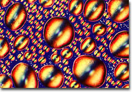
Nickel Oxide on Indium Phosphide The earliest studies of magnetic thin films took place in the late nineteenth century. August Kundt was a pioneer in the field who created thin films of iron, nickel, and other materials, and studied the dispersion of light passing through these films. The optical properties of ferromagnetic films remained their chief interest to researchers until the 1950s, when increasing attention to computer technology turned the tide, and the films began to be considered in terms of their potential for information storage. As early as 1960, the development of thin film memory had been formally announced and by 1962 it was available commercially in the UNIVAC 1107, which utilized the new material for its 128-word general register stack. The rest of the machine's storage was provided by the more primitive and less expensive technology of ferrite cores. Developed by the Sperry Rand corporation with the aid of governmental financial support, early thin film memory was constructed by depositing dots of permalloy, an iron-nickel alloy, onto small glass plates utilizing a mask and vacuum evaporation techniques. Connections took the form of etched, multilayer circuits placed on the permalloy dots. 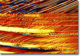
Iron Oxide on Magnesium Oxide In recent years, magnetic thin film systems have become much more complex than they were in the early years of the field, as society has come to expect smaller and faster kinds of technological equipment. Magnetic thin films are now frequently utilized as part of multilayered structures rather than independently. These layered systems may include non-magnetic materials and other components as well as magnetic films, often resulting in structures with unique properties. Ongoing research and work with these structures have facilitated the discovery of many new kinds of physical processes, including interlayer exchange coupling (IEC) and giant magnetoresistance (GMR). First recognized in 1986, IEC is an interaction that occurs between two ferromagnetic layers divided by a nonmagnetic metallic spacer layer that causes the layers to align either ferromagnetically or antiferromagnetically when exposed to an external field. In such cases, the extent of the coupling is related to the thickness of the spacer. Discovered a few years after IEC, the GMR effect is characterized by very large resistance changes in a multilayer system when a magnetic field is applied. Studies of both IEC and GMR have ballooned into entirely new academic fields, such as magnetoelectronics and spin electronics, and have also spawned the development of a number technological advances. 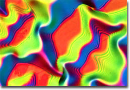
Nickel Oxide on Magnesium Oxide The GMR effect has played a particularly important role in modern applications of magnetic thin films. Indeed, the phenomenon has been found to make magnetic thin film systems that exhibit it to be extremely well suited for sensors. The first technologies to harness the power of the GMR effect were developed by IBM, who in 1994 announced the creation of the industry's most sensitive sensor for detecting computer data on magnetic hard disks, an achievement made possible by the GMR effect. Within three years, the company introduced the sensors into their hard disk drives for desktop computers, and the pioneering GMR products were a great success. It did not take long for the advantages of GMR-based sensors, which include increased sensitivity to magnetic fields from disks and a decrease in electronic noise, to become apparent. Indeed, within a few years of IBM's initial production of the innovative new disk drives, GMR-based technologies became dominant in the drive sensor industry. Moreover, current trends seem to suggest that eventually thin film structures that exhibit the GMR effect may find their way into the market in a mounting number of arenas, possibly appearing in items such as antilock brakes, electrical safety device sensors, transformers, traffic monitors, alarm systems, and metal detectors. |
© 1995-2025 by Michael W. Davidson and The Florida State University. All Rights Reserved. No images, graphics, software, scripts, or applets may be reproduced or used in any manner without permission from the copyright holders. Use of this website means you agree to all of the Legal Terms and Conditions set forth by the owners.
This website is maintained by our
|