The Sunset 2 Chip
|
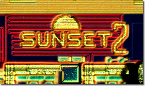
This silicon sunset was discovered on a chip designed to military specifications for use in 594/637 class submarines during the late 1980s. The chip was extracted from some Navy electronics sold at surplus, although we don't know the exact nature of the equipment that used this chip. Because the sunset has a "2" designation, we assume that there was an original Sunset ("1") chip. Russ Chmela and Scott Lewis, formerly of IBM Microelectronics, inform us that the Sunset 2 chip is a 72K (8K x 9) DRAM and the older brother of a short-lived Sunset 1, a 36K (4K x 9) DRAM chip. Scott, who designed the Sunset 2 logo, was the team leader on the original Sunset 1 chip design, which began in June of 1973, with the first chips shipping a year later. The integrated circuit was built using a metal gate/silicon plate process that produced lower yields than the silicon gate process subsequently adopted by the industry. The Sunset 2 chip is a double dense version of the Silicon 1 that was designed in 1976. Scott informs us that both of these wide-byte chips were targeted for printers and terminals. Because this chip was developed for commercial computing, and Russ and Scott were surprised that it was found in a military application. |
© 1995-2025 by Michael W. Davidson and The Florida State University. All Rights Reserved. No images, graphics, software, scripts, or applets may be reproduced or used in any manner without permission from the copyright holders. Use of this website means you agree to all of the Legal Terms and Conditions set forth by the owners.
This website is maintained by our
|