Lattice Forest
|
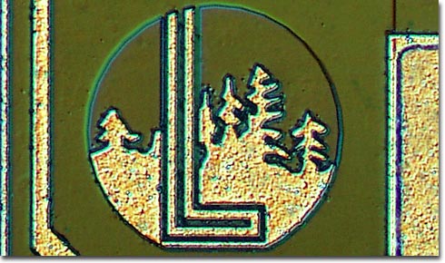
A small group of trees, perhaps the beginning of a forest, was photographed near the pad ring of a Lattice Semiconductor GAL20V8 programmable logic device. This chip combines high performance CMOS technology with electrically erasable floating gate features to produce a high speed device that has revolutionized the PLD industry. The artwork on this chip was designed by Ken Campbell, a mask designer for Lattice who has been with the company since it was founded in 1983. The image depicts one of Lattice's early logos and represents a silicon wafer backdrop with a forest in the foreground to emphasize the emergence of Lattice Semiconductor from the "Silicon Forest" of chip manufacturers. In 1984, Lattice Semiconductor applied for and received the trademark for use of the name Silicon Forest. The chip containing this artwork was loaned to us by Chipworks, a company that is an international provider of reverse engineering services, analyzing the circuitry and physical composition of semiconductor chips and electronics systems for competitive study, intellectual property support, and reliability assurance. |
© 1995-2025 by Michael W. Davidson and The Florida State University. All Rights Reserved. No images, graphics, software, scripts, or applets may be reproduced or used in any manner without permission from the copyright holders. Use of this website means you agree to all of the Legal Terms and Conditions set forth by the owners.
This website is maintained by our
|