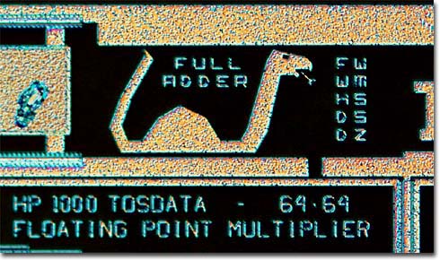
The Full Adder
|
This cute little snake was found tucked into the pad ring of a Hewlett-Packard math chip, the HP 1000 Tosdata 64-bit floating point multiplier. The chip is a member of a set of arithmetic integrated circuits that contain various puns on addition circuits. The engorged snake was placed onto the chip to represent the "full adder", a common logic circuit that takes three binary bits and adds them together resulting in a summation with a carry digit. There is another chip in this set that is represented by the "half adder", a logic circuit that sums two input bits. Just for the record, an Adder is also a poisonous snake found in Europe, Australia and New Guinea. Manufacturing a SOS chip begins with a sapphire wafer. The chemical composition of sapphire is aluminum oxide (Al2O3), made from ions of aluminum and oxygen. In wafer form, sapphire is a light gray semi-transparent material that is very tough and rugged. Silicon is grown onto the smooth, hard, glass-like surface of the sapphire wafer using epitaxial methods such as Molecular Beam Epitaxy (MBE) or Metal Oxide Chemical Vapor Deposition (MOCVD) where the silicon atoms are assembled one-by-one on the surface of the sapphire wafer. Because the crystal structure of silicon is similar to sapphire, the SOS structure appears to be one crystal with a strong molecular bond between the two materials. The silicon is then patterned into transistors (see our tutorial on Building A Transistor) and the circuit is completed using normal processing. Initially the SOS technology was developed back in the 1960s for use in military and aviation applications requiring high temperature and "radiation hardened" chips. The main commercial promise of a sapphire substrate is that it has very low capacitance compared to silicon, allowing signals to pass overhead in wires without slowing down. It also allows N- and P- type transistors to be packed closer together, an improvement in density over silicon CMOS (standing for Complementary Metal-Oxide Semiconductor, a MOS circuit formed with both N-channel and P-channel transistor devices). HP took advantage of these features during the evolution from "LSI" to "VLSI" (Large Scale Integration and Very Large Scale Integration) chips in the late 1970s/early 1980s. The math chips and related CPU chips from HP were among the first "VLSI". (a new term at the time) Silicon manufacturing advanced faster than sapphire, and the SOS process faded from use in commercial applications. It has always maintained a niche in military applications and has seen a recent surge of interest in micromachined sensors. There is also a lot of research in the area of "Silicon-on-Insulator" where the insulator is silicon dioxide (SiO2, glass) instead of sapphire. SOI processing stays much closer to the bedrock of silicon technology. |
© 1995-2025 by Michael W. Davidson and The Florida State University. All Rights Reserved. No images, graphics, software, scripts, or applets may be reproduced or used in any manner without permission from the copyright holders. Use of this website means you agree to all of the Legal Terms and Conditions set forth by the owners.
This website is maintained by our
|