
Spike (M.I.) Walker
Etched Silicon Wafer
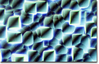
English photomicrographer Spike (M.I.) Walker has been a consistent winner of the Nikon Small World competition for many years and has published many articles and a book about microscopy. Featured below is a photomicrograph of an etched silicon wafer.
|
The underside of a silicon wafer, utilized in the manufacture of integrated circuits, was etched and photographed with reflected light. The objective was an epiplanachromat 16x/0.35 NA (polarized light) utilizing a vertical illuminator (epicondenser) and differential interference contrast (DIC) illumination. The microscope was a Zeiss Ultraphot III with a automatic 35-millimeter photohead. The film was Fujichrome Velvia. (63x) |
Silicon is an abundant element most commonly found in sand, as the oxide silicon dioxide. Before it can be made into an integrated circuit, the raw silicon material must be very pure. Silicon is refined from ordinary sand, Then melted and grown into ingots through a process that resembles dripping candles, which are 99.99999999 percent pure! Wafers are then sliced from the ingots and baked to sterilize and smooth their surfaces prior to being placed into fabrication assembly lines to produce integrated circuits. Working with silicon to build chips is done only in "clean rooms" where near-sterile conditions exist, because it takes only a single microscopic dust particle to contaminate a wafer, making that part of it defective.