|
For years, chip designers have etched drawings and initials onto unused corners of silicon chips as a means of signing their work. Recently, a researcher at Florida State University (FSU, Tallahassee, FL; 850-644-0542) who specializes in photomicrography has unveiled these micron-sized chip pictures and showcased them as part of his 70,000-image online gallery. He now funds his 18-person lab with revenues from the images, which include magnified buckyballs, polymers, and superconductors. His gallery also features nine interactive virtual microscopes.
The Photomicrography Gallery
Creating Chip Designs
Applications For Semiconductor Art
Other Gallery Collections
Virtual Microscopes
The Photomicrography Gallery (Back to Top)
Microscopic art galleries grace the chip-lined interiors of most electronic devices. Etched on unused sections of silicon chips, minute images of buffalo herds, hummingbirds, and other characters form a collection of hidden artistry among the jungle of wires. Created by circuit designers, the drawings form unique signatures that pass unseen by the millions who use devices driven by the chips. Michael Davidson, senior research engineer at FSU, has created an online gallery featuring these and approximately 70,000 other photomicrography images.
Although Davidson began as a biophysicist at the nearby National High Magnetic Field Laboratory, he has evolved into an online pop artist, of sorts; a connoisseur who uncovers microscopic chip artistry through his image-packed Web site (http://micro.magnet.fsu.edu/creatures/index.html). Recently, he added a section to his site that explains the technical details behind the search for silicon doodles. He has also developed an interactive Java tutorial that shows how drawings are created on chips.
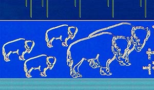
The Focus II Math chip, a Hewlett-Packard 64-bit combinatorial divider, featured this herd of buffalo. The chip was created by the HP chip-design team in Fort Collins, CO. The buffalo are the mascot of the University of Colorado.
Davidson's photomicrography project began as part of a NIH-funded research program to photograph DNA strands. After expanding his subject repertoire and perfecting several lighting techniques, Davidson found that his work was marketable outside the research arena. He now earns approximately $500,000 each year from image licensing fees and magnified product shots for corporate clients like Intel. This commercial revenue stream allows him to pursue projects that he feels are important or interesting without justifying them to funding agencies. His lab now employs 18 people who magnify and photograph subjects like vitamins, proteins, materials, and semiconductor chips. His collection includes 70,000 photographs.
�We use high-end optical microscopes to enlarge all sorts of things so that we can photograph them,� Davidson says. Semiconductor chip drawings are his newest passion. �We're actively searching for chip critters now, but the chips often have to be pried from the boards, which is difficult.� To do this, Davidson's team bakes each board at 525 degrees Celsius for 12 hours. This turns the glue into a powdery ash, allowing the chips to be rooted from their foundations.
�We have about 75 creatures posted online, and have been posting a new one each day for some time now,� Davidson says. He plans to write a book when he has accumulated 300 chip images. �We chase every lead that we get about images on chips. I've spent about $10,000 buying chips to scan since January 1999.�
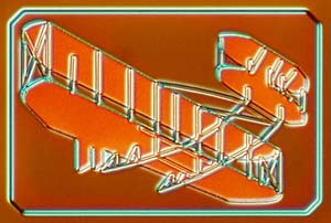
This rendition of the original Wright brothers' biplane was discovered on an early 1980s era NCR Microelectronics memory integrated circuit, loaned to Davidson's lab by Greg O'Hara of Marietta, GA. The wingspan of this silicon biplane is 200 micrometers, about 1/60,000 the size of the original plane.
As the example above shows, Davidson doesn't buy every chip that his team photographs. Instead, they scavenge discarded or borrowed electronics for new chips to search. Scanning a chip for images is very time-intensive; it can take months to analyze a chip. Results are not guaranteed because each chip does not hold an image. In some cases, the search pays off—Daffy Duck's likeness was found on the MIPS R4400 processor weeks after Waldo's image was discovered, even though both were on the same chip.
Creating Chip Designs (Back to Top)
�Creating a chip is a bit like creating a book by hand-writing each page,� says Dan Zuras, a chip designer at Hewlett-Packard Co. (Palo Alto, CA). Zuras has created chip images such as a roadrunner and a crossword puzzle that incorporates the names of his design team members. �When you do time-intensive projects like designing chips, it's nice to add something to represent the labor that was involved. It's like the illuminations in early hand-written copies of the Bible.�
Designers often create increasingly complex drawings with each chip they develop, producing images that incorporate different colors and textures. Since Davidson's chip zoo site was launched in October 1998, this artistic effort has received an extra boost. Through Davidson's site, chip designers can now see their colleagues' doodles, and their own, for the first time, says long-time chip artist Kevin Kuhn, mask layout designer for Silicon Graphics International (Mountain View, CA).
Now that he can see images from other designers, Kuhn says that he has begun trying new techniques to create unique chip images. Of the images he has created, his favorite is an intricate California license plate with the chip name and palm trees etched on it. �I use three metal layers on the chips to add depth and shading to my drawings,� Kuhn says. �I can now create a drawing in a few hours because I have done so many of them.�
Chip-drawing software makes it relatively simple to create chip designs, Kuhn says. Developed during coffee breaks and after work, the images are often created to represent some element of the chip's name or the group who developed it, says Willy McAllister, MEMS project manager at Hewlett-Packard Co. (Palo Alto, CA) and chip artist. Because chips are often nicknamed after predators, there are a large number of cat, snake, and dinosaur images.
�When we realized that it was just as easy to draw creatures as it was to draw transistors, we started picking project names that would produce excellent doodles,� McAllister says. �The drawings are executed by whomever wants to stay late and do them.�
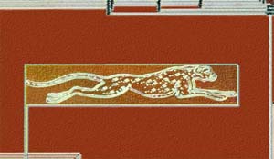
This cheetah races across the surface of a Hewlett-Packard memory controller integrated circuit. The chip was designed in combination with a very early HP-PA microprocessor that was code named Cheetah and used in the HP-900/750/755 series computers. Willy McAllister helped create the image.
All of the images follow strict guidelines. Every piece of metal on each chip must be connected to a device or power source, or grounded. If chip doodles do not follow this rule, production may be halted to identify the source of the error. Images must also bear a cohesive look so that quality inspectors can recognize the drawings without being confused by any of their elements.
Production at one chip-manufacturing company was slowed once by an image of a cheetah that was created by drawing an outline on one metal layer and spots on another, McAllister says. When viewed from above, the image was an integrated animal. When the chip was inspected layer by layer, production was halted because the unconnected spots were thought to be flaws. Halting chip production could cost a company more than $500,000 a day, Zuras says.
�The practice is actually quite dangerous in a business sense,� McAllister says. �The doodles don't look like normal circuitry and checking tools get confused by them. There are cases where the first prototype of a new chip was ruined by a poorly drawn creature, delaying the introduction of a product by several months.�
Although accidents may occur, instances in which product lines are impaired by doodles are exceptionally rare, Kuhn says. McAllister, Zuras, and Kuhn all agree that they create a drawing only after verifying and reverifying that it will not damage the chip's functionality.
Silicon Graphics and Hewlett-Packard Co. don't encourage their employees to create chip doodles, although they tolerate the artistry. Other companies are not as tolerant. Intel does not allow its designers to create any drawings on its chips, although Davidson says he just received a tip about an image on an Intel processor. He has not found any images on chips designed and produced in Japan.
Applications For Semiconductor Art (Back to Top)
Created primarily for artistic enjoyment, chip doodles occasionally serve a useful functions as well, Kuhn says. Silicon Graphics chip debuggers use his images as landmarks when they search for specific pieces of circuitry. �We have plots of the circuitry that are blown up to 15-ft by 15-ft, but you lose all sense of your surroundings when you zoom in with a high-power microscope,� Kuhn says. �The drawings give some sense of perspective to locate specific parts of the chip.�
Although most chip artists scoff at the idea of long-term practical uses for their doodles, Zuras suggests that the technique might eventually be used to inscribe holograms on chips. When a laser is shone on one of these, it could project a pattern smaller than the wavelength of light. Despite the possibility of this application, Zuras says that the concept is hypothetical and has only a tenuous connection to chip doodling.
Without a significant application, semiconductor art remains a hobby for designers who create the images to give their chips a personal touch. Although Davidson's online chip art gallery has piqued interest in this unique pastime, some believe that fewer chips are being etched today than there were 20 years ago. This is thought to be due to a decrease in the involvement that designers have with each chip, a result of larger design teams and more complex chips. �When the relationship between the designer and chip is less personal, it's less likely that they will take the time to create an image on it,� Zuras says.
Other Gallery Collections (Back to Top)
Whether or not the frequency of chip images has decreased, Davidson continues to hunt. While his semiconductor art collection grows, so do the other areas of his online photo gallery (http://www.microscopy.fsu.edu/micro/gallery.html). The site includes images of polymers, dinosaur bones, ice cream, and the �cocktail collection,� a group of magnified alcoholic beverage images. One of his most popular projects, the cocktail collection has been licensed by Stonehenge, a major New York designer, for use in gentlemen's ties—Davidson has earned over $1 million from royalties earned through this arrangement.
More than 100 drink mixtures are featured in Davidson's Cocktail Collection—including this image of this Mint Julip. To date, more than $900,000 has been donated to Mothers Against Drunk Driving as a result of cocktail necktie sales.
�At first we chose subjects based on availability,� Davidson says. �Our philosophy is to build entire collections along a motif rather than taking random images like other photographers. We do this no matter what it takes—it took me five years to photograph all of the vitamins.� His photo gallery now includes more than 50 collections.
In addition to these images, Davidson's team also assists in some scientific pursuits. His team frequently takes photographs of new materials developed at the nearby National High Magnetic Field Laboratory. These images can reveal tiny cracks in new magnetic materials, pinpointing trouble before it occurs.
Virtual Microscopes (Back to Top)
Davidson's microscopic explorations also have an educational, interactive flair to them. His site features a comprehensive online microscopy primer filled with information about the functions and components of all types of microscopes. Working with representatives from Olympus (Tokyo), he has developed nine virtual microscopes that can be manipulated from anywhere in the world.
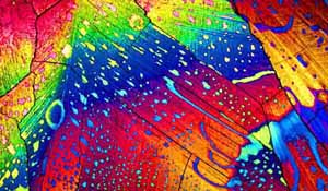
This magnified buckyball thin film is shown on a silver substrate.
�We're not doing pioneering work in microscopy, we're making art and teaching usage,� Davidson says. �As far as science is concerned, we're trying to put an artistic twist on research objects such as magnets, buckyballs, and other things to give science new insight.�
The virtual microscope controls do not actually focus microscopes in Davidson's lab. Instead, they each imitate a different type of microscope as it examines predetermined samples. Users can move the samples and focus the microscopes through a Web interface. A mix of Java and photomicrography allows Davidson to use six images to show a full sample rotation, instead of the 18 that would be required if Java were not employed—speeding the simulation. The virtual microscopes are being used at FSU and 35 other universities, Davidson says.
Although these accomplishments have propelled Web-based education, they are not likely to ever be the areas for which Davidson is most well known. His new perspective on the microscopic world has gathered him a devoted audience of fans, helping him to expand his lab and trailblaze new techniques in photomicrography, an area that seems to have taken on a life of its own. From cocktails to chip critters, his virtual gallery seems to be virtually limitless.
For more information, call 850-644-0542 or e-mail eclark@magnet.fsu.edu.
By Laura Vandendorpe
|