
Integrated Circuit Image Gallery
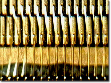
Intel 486DX2 Microprocessor
As the quest for the computation crown continued into Intel's fourth generation of microprocessors, the 486 family grew with the use of internal clock doublers and triplers, creating the then-"speed demon" DX2s and DX4s. In March 1992, the 486DX2 was released with an external clock (bus) speed of just 25 MHz, but with a "lightning fast" internal clock speed of 50 MHz.
View a second image of the Intel 486DX2.
View a third image of the Intel 486DX2.
Capable of executing 41 million instructions per second (MIPS) by using 1.2 million transistors, the Intel 486DX2 was fabricated with 0.8-micron silicon technology on an 81-square millimeter wafer. The DX2 chip featured 8 Kbytes of cache memory, support of 4 Gbytes of addressable memory, and an integral 80-bit floating-point unit (FPU). The 32-bit (internal register and external bus widths) central processing unit (CPU) was followed up in August 1992 with the faster 66 MHz (internal clock speed) 486DX2. This newer model operated on 5 volts and had a peak power dissipation of 7.0 watts, but more typically ran at a cooler 4.9 watts.
Like its slower, older pin-compatible 486DX and SX family members, the DX2s were complete instruction set computing (CISC) specific processors. Intel created the new and upgrade processor markets for new and existing personal computer users by applying their innovative clock doubling technology and their newly refined silicon chip manufacturing techniques. Manufacturers embraced these marketing and packaging moves, because it allowed them to sell newer and faster motherboards and personal computers without the expense of complete hardware redesigns. This was the kind of economic edge the company was seeking against 486 clones and other microprocessor makers during the wide-open home and business computer era of the early 1990s. The downside of the engineering design for the 80486DX2 microprocessor was that external operations still occurred at the lower clock speed, and memory accesses, and transfers to and from input/output devices were much slower than internal chip operations, creating computing bottlenecks. Despite these problems, the 486DX2 was widely successful in its day.
Contributing Authors
Omar Alvarado, Thomas J. Fellers and Michael W. Davidson - National High Magnetic Field Laboratory, 1800 East Paul Dirac Dr., The Florida State University, Tallahassee, Florida, 32310.
BACK TO THE INTEGRATED CIRCUIT IMAGE GALLERY
BACK TO THE DIGITAL IMAGE GALLERIES
Questions or comments? Send us an email.
© 1995-2022 by Michael W. Davidson and The Florida State University. All Rights Reserved. No images, graphics, software, scripts, or applets may be reproduced or used in any manner without permission from the copyright holders. Use of this website means you agree to all of the Legal Terms and Conditions set forth by the owners.
This website is maintained by our
Graphics & Web Programming Team
in collaboration with Optical Microscopy at the
National High Magnetic Field Laboratory.
Last Modification Friday, Nov 13, 2015 at 02:19 PM
Access Count Since September 17, 2002: 8011
Visit the website of our partner in introductory microscopy education:
|
|