The Superlattice Collection
Nickel-Copper On Mica
Superlattices
|
Artificial metallic superlattices are multilayered thin films, prepared by alternately depositing two or more elements using vacuum deposition or sputtering techniques. The concept of the superlattice was originally developed by physicists Leo Esaki and Raphael Tsu, who were both working at the IBM T. J. Watson Research Center in the 1960s. By 1969, the pair had jointly created a semiconductor superlattice, initiating a new field of research in man-made crystals. The invention of Esaki and Tsu is generally believed to mark the first production of a new semiconductor material through use of the advanced growth technique of molecular beam epitaxy (MBE). This technique is characterized by the growth of thin films through the exceedingly slow evaporation of semiconductors or metals in a clean environment. The deposition rate achieved with MBE is generally only a few nanometers per minute. Also, when the technique is utilized to grow metals rather than semiconductors, evaporation sources must operate at significantly greater temperatures. The other primary method traditionally utilized for constructing superlattices is known as metal-organic chemical vapor deposition (MOCVD), a process that involves the use of chemical reactions to create thin films of material on a substrate. 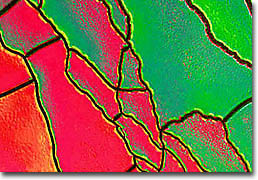
Iron-Nickel Oxide Throughout the 1970s and 1980s, Esaki and his coworkers continued their groundbreaking efforts, while at the same time instigating a broad range of investigations carried out by other research groups. Over time, continued studies of superlattices helped reveal a variety of related phenomena for the first time, such as high electron mobilities, large Stark shifts, and differential negative resistance, in addition to paving the way for practical superlattice-based technologies. Work in the field is still in progress, but superlattice structures have already begun to be utilized in field effect transistors to increase the current carrying capacity of the devices and, consequently, the output power. Superlattices also find use as photodetectors and as components in a new variety of light-emitting diodes. The multilayered thin films are of great interest as well due to their promise for the synthesis of new materials, particularly in the rapidly growing semiconductor field. 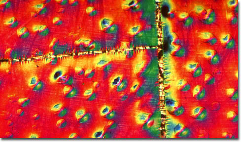
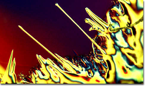
Gold-Nickel on Mica Some of most interesting applications of superlattices to date include their inclusion in lasers, such as the quantum cascade laser invented in 1994 by a research team at Bell Labs, a branch of Lucent Technologies. This unique device is fundamentally different from other semiconductor lasers, operating, in essence, as if it were an electronic waterfall, electrons cascading down a sort of energy stairway and emitting a photon at each step along the way. Due to this cascading photon emission, quantum cascade lasers are inherently more powerful than other laser types, such as diode lasers. The superlattice-based devices are also distinguished by their high level of reliability as well as the fact that their wavelength is determined by the thickness of the layers in the superlattice instead of their material composition, which enables the laser to cover the entire mid-infrared spectrum with a single combination of materials comprising the superlattice. The quantum cascade laser is still being perfected, but may someday be highly useful in areas such as the remote monitoring of environmental pollution, collision-avoidance radar, and medical diagnostic tools. 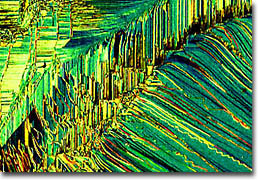
Iron/Nickel Oxide on Magnesium Oxide An important consideration in the fabrication of superlattices is finding materials that are good lattice matches. This is because if the spacing between atoms in the substrate is too different from that of the overlying crystal, then the top crystal may exhibit wrinkling or other deformities. The surface of a perfect superlattice, however, resembles a mirror, its texture appearing smooth and flawless when examined using optical microscopy. The metallic superlattices depicted in this collection are composed of alternating layers of metallic thin film. The wrinkling seen in many of the accompanying photomicrographs is caused by poor adhesion of the films to the substrate or a severe lattice mismatch. Thus, from a structural point of view, metallic superlattices can be divided into two groups. The first category is epitaxial superlattices in which alternating layers of metals provide a good epitaxial lattice match for the successive layers and the growth of a single crystal superlattice is possible. The second category encompasses superlattices in which an epitaxial relationship cannot be maintained and each layer can possess a different structure. Although these systems are far less regular than the epitaxial superlattices, even when each layer is amorphous the superstructure can still be established. 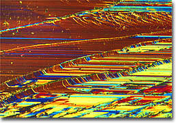
Iron/Nickel Oxide on Magnesium Oxide A wide spectrum of elements and compounds are suitable for deposition into superlattice structures, and the range of properties displayed by the resulting superstructures is greatly dependent upon the properties of both individual lattices as well as the interaction between them. For example, superlattices composed of magnetic and non-magnetic materials behave differently than the bulk materials and demonstrate a multiplicity of couplings between the magnetic layers. These couplings can be manipulated by choosing different layer materials and modifying their thicknesses. Through such control of superlattice properties, engineers have been able to drastically improve the performance of certain devices, such as high-performance magnetic recording heads and sensors. Yet, the magnetic fluctuations, known as magnons, that occur in superlattices composed of layered magnetic and non-magnetic materials is not fully understood. Through further studies, however, scientists hope to come to a more complete comprehension of the magnetic interactions that take place in such materials as well as the distinctive couplings that occur between layers. |
© 1995-2025 by Michael W. Davidson and The Florida State University. All Rights Reserved. No images, graphics, software, scripts, or applets may be reproduced or used in any manner without permission from the copyright holders. Use of this website means you agree to all of the Legal Terms and Conditions set forth by the owners.
This website is maintained by our
|