|
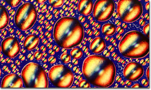
A variety of methods for creating thin films have been developed over the years, but the basic technique involves firing a high-temperature beam of molecules into a vacuum chamber. Inside the chamber, the beam comes into contact with a substrate, such as a wafer of silicon, lanthanum aluminate, indium phosphide, or a similar substance. Under the proper conditions, the incoming molecules will organize themselves into a thin, perfect crystalline layer on the wafer’s surface, but creating the appropriate conditions is no easy task. If the molecules of a thin film do not crystallize perfectly, the film is of no practical use, but may still yield important clues as to how the process of creating thin films may be improved in the future. In the image shown above, molecules of nickel oxide are found on an indium phosphide substrate, but instead of forming a thin sheet during the deposition process, they have bunched up into bubbles, rendering the sample unusable for most purposes, but, nevertheless, strangely beautiful under the microscope.
|
